
- Semiconductor Devices - Home
- Introduction
- Atomic Combinations
- Conduction in Solid Materials
- Conductivity & Mobility
- Types of Semiconductor
- Doping in Semiconductors
- Junction Diodes
- Depletion Zone
- Barrier Potential
- Junction Biasing
- Leakage Current
- Diode Characteristics
- Light Emitting Diode
- Zener Diode
- Photo Diode
- Photovoltaic Cells
- Varactor Diode
- Bipolar Transistors
- Construction of a Transistor
- Transistor Biasing
- Configuration of Transistors
- Field Effect Transistors
- JFET Biasing
- Semiconductor Devices - MOSFET
- Operational Amplifiers
- Practical Op-Amps
- Semiconductor Devices - Integrator
- Differentiator
- Oscillators
- Feedback & Compensation
Semiconductor Devices Tutorial
Semiconductor Devices Tutorial
Semiconductor Devices are the circuit elements made up of a material which is neither a conductor nor an insulator, and are used for designing electronic circuits and systems. The material which has properties lying between a good conductor and a good insulator is called a semiconductor. Semiconductor devices are widely used in a number of electronic circuits and applications because of their small size, longer lifespan, modular design, higher reliability, and cost effectiveness.
Semiconductor devices are found as the discrete components in all electronic devices and systems. These devices are becoming popular in circuits and systems ranging from microelectronics to power electronics because of their wide range of current and voltage handling capabilities. Semiconductor devices can typically handle currents within a range of a few nA to more than 5 kA, and voltages higher than 100 kV.
Another important thing best about semiconductor devices is that they can be integrated into complex but easily manufacturable electronic circuits, referred to as ICs (Integrated Circuits).
This tutorial is meant for explaining the functional operation of semiconductor devices, explaining the operation of these devices in a circuit, etc. Each topic in this tutorial is explained well using circuit diagrams for better understanding.
After completing this tutorial, students or readers will be at a moderate level of expertise to explain the basics related to semiconductor devices.
What are Semiconductors?
Those engineering materials which have a conductivity (or resistivity) between conductors (metals) and insulators are called semiconductors. These materials are widely used for making electronics devices like diodes, transistors, SCRs, etc.
Semiconductor materials can be present either as pure elements like silicon, germanium, etc. or as compounds like gallium arsenide.
Semiconductor materials are broadly classified into the following two main types −
- Intrinsic Semiconductors − Semiconductors in their purest chemical form and exist as a single element are called intrinsic semiconductors. Examples of intrinsic semiconductors include silicon, germanium, etc.
- Extrinsic Semiconductors − Semiconductors obtained by adding impurities into the pure semiconductors to enhance their conductivity are known as extrinsic semiconductors. Gallium Arsenide is an example of extrinsic semiconductor.
Extrinsic semiconductors are further classified into two types namely, N-Type Semiconductors and P-Type Semiconductors.
Properties of Semiconductors
Here is a list of some of the important properties of semiconductors −
- Semiconductors have the resistivity between 10-5 m and 106 m, and conductivity between 105 mho/m and 10-6 mho/m.
- Semiconductors have a negative temperature coefficient of resistance. Hence, the resistance of semiconductors decreases with the increase in temperature.
- In semiconductors, the current flow takes place because of both electrons and holes.
- At 0 Kelvin temperature, semiconductors become insulators.
- Semiconductors have lower power losses when using for energy conversion, switching, etc.
Some Common Semiconductor Materials
This section provides a brief introduction to some most commonly used semiconductor materials −
- Silicon (Si) − It is the most commonly used semiconductor material for manufacturing semiconductor devices. It is very popular because of its low cost, simple processing, and wide temperature range.
- Germanium (Ge) − Germanium is the second most widely used semiconductor material in electronic devices. Today its use become less than silicon due to its thermal sensitivity. However, it is being used by alloying with silicon to manufacture very high-speed SiGe devices.
- Gallium Arsenide (GaAs) − GaAs is also used for manufacturing high-speed semiconductor devices. However, it is more expensive to produce GaAs devices due to its small wafer size limitation.
- Gallium Nitride (GaN) − GaN is a semiconductor material having high strength and thermal conductivity. Hence, it is being widely used for manufacturing high-power devices such as power ICs, LEDs, radio frequency components, etc.
- Silicon Carbide (SiC) − SiC is also used in certain semiconductor devices as a raw semiconductor material. It is mainly used in devices which are designed for operating in high temperatures and ionizing radiation environments. Some common examples of devices fabricated from SiC include power ICs, IMPATT diodes, and blue LEDs.
What is a Semiconductor Device?
A semiconductor device is a type of electronic device made up of a semiconductor material like silicon, germanium, gallium arsenide, or any organic semiconductor material and whose operation depends on the electronic properties of these materials.
Semiconductor devices conduct electric current in the solid state, instead of as free electrons in metals and ions in ionized gases. These devices can be manufactured as either a single discrete device or an integrated circuit consisting of multiple devices in a single unit.
Current conduction in semiconductor devices mainly occur due to mobile charge carriers called free electrons and holes. A semiconductor device which is manufactured by using N-type semiconductor has negative charges, i.e., electrons as the majority charge carriers, and device which is manufactured by using P-type semiconductor has positive charges i.e., holes as the majority charge carriers.
MOSFET (Metal Oxide Semiconductor Field Effect Transistor) is one of the most common semiconductor devices used across the world. Other semiconductor devices include BJT, diode, SCR, IGBT, UJT, and thousands more.
Main Types of Semiconductor Devices
There are thousands of semiconductor devices available today. A brief introduction to some of the main semiconductor devices is given here −
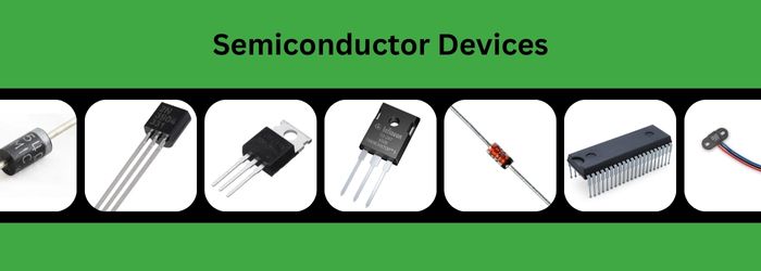
Diode
Diode is a two-terminal semiconductor device, having a p-n junction. Hence, it is also known as a p-n junction diode. It is formed by joining a p-type semiconductor with an n-type semiconductor material. At the junction, it has a depletion region that prohibits the movement of charge carriers across the junction. The diode works as follows −
- When the p-side terminal is connected to a higher electric potential and the n-side terminal is connected to a lower electric potential, the depletion region diminishes and allows the movement of charge and hence the flow of current through the diode. This is called forward biasing of the diode. The diode acts as a closed switch.
- Opposite to this, when p-side is connected to a lower potential with respect to the n-side, the depletion region becomes wider and restricts the movement of charge across the junction and hence no current flows through the device. This condition is called reverse biasing of the diode. The diode acts as an open switch.
Bipolar Junction Transistor (BJT)
BJT is a three-terminal semiconductor device, having two p-n junctions. It has three semiconductor regions namely emitter, base, and collector.
The operation of a BJT depends on its configuration in the circuit, which is briefly described here −
- When one junction of the BJT is forward biased (mainly emitter-base junction) and the other junction (base-collector) is the reverse biased, the BJT operates in the active region and acts as an amplifier.
- When both junctions of the BJT are forward biased, the device operates in the saturation region and acts as a closed switch.
- When both junctions of the BJT are reverse biased, the device operates in the cut-off region and acts as an open switch.
Hence, a BJT is used for two purposes namely, amplification and switching of signals in a variety of electronic devices.
Field Effect Transistor (FET)
FET is another type of transistor, having three terminals namely, Source (S), Gate (G), and Drain (D). In FETs, the flow of electric current though the device is controlled by using an electric field. Field effect transistors are widely used in computer ICs and memory chips.
FETs are further classified into two types namely, Junction Field Effect Transistors (JFETs) and Metal Oxide Semiconductor Field Effect Transistors (MOSFETs).
Insulated-Gate Bipolar Transistor (IGBT)
IGBT is a three-terminal semiconductor device used in high power applications for switching purposes. IGBT has three terminals namely, Emitter (E), Gate (G), and Collector (C). It consists of a structure of four alternating semiconductor layers namely NPNP with a MOS (Metal-Oxide Semiconductor) gate structure. It is primarily used in applications where fast switching with high efficiency is desired like in VFDs, UPS, etc.
Silicon Controlled Rectifier (SCR)
SCR is a power semiconductor device having three terminals namely anode, cathode, and gate. It has four alternate layers of n-type and p-type semiconductors, structured as PNPN, where the outer P layer forms the anode and the outer N-layer forms the cathode. The inner P-layer is connected to the gate terminal.
Being a power semiconductor device, SCR finds its applications in high power and high voltage circuits like in inverters, motor control circuits, power regulators, lamp dimmers, etc.
Advantages of Semiconductor Devices
Semiconductor devices offer several advantages over mechanical and electromagnetic devices, some key of them is listed here −
- Semiconductor devices have a highly compact size.
- Semiconductor devices consume less power and hence more energy efficient.
- Semiconductor devices do not involve any mechanical movement; hence they have high-speed operations.
- Scalability and mass production of semiconductor devices is easier.
- Due to absence of moving components, semiconductor devices are more durable and reliable.
- Semiconductor devices are versatile. For example, a transistor can be used for amplification as well as switching purposes.
- Semiconductor devices can be manufactured in the form of complex integrated circuits and hence they are space efficient.
Disadvantages of Semiconductor Devices
Apart from the advantages, semiconductor devices also have certain disadvantages as listed below −
- Semiconductor devices are highly sensitive to temperature variations, and high temperatures can degrade their performance or cause failure.
- Semiconductor devices have limited tolerance in terms of power handling capacity.
- The initial cost of designing and manufacturing semiconductor devices is significantly high.
- The performance of semiconductor devices degrades over time due to aging and they need to be replaced after a certain point of time.
- Semiconductor devices can be damaged permanently due to electrostatic discharge.
- The fabrication process of semiconductor devices is highly complex and resource intensive.
- Most semiconductor devices are non-repairable and has to be replaced if malfunction.
Applications of Semiconductor Devices
Semiconductor devices find numerous applications, ranging from microelectronics to power electronics. Some common examples highlighting the applications of semiconductor devices are given below −
- Semiconductor devices like transistors and diodes are used as the building blocks of digital logic gates.
- Semiconductor devices are used for designing digital circuits like counter, registers, memory devices, etc.
- Semiconductor devices are also used in microprocessors and microcontrollers.
- Semiconductor devices are used to design analog circuits like amplifier, oscillators, rectifiers, etc.
- Semiconductor devices are also employed in designing mixed-signal circuits.
- Semiconductor devices having high power handling capacity are used in high current and voltage applications like SMPS, motor control, VFDs, etc.
What You Will Learn in Semiconductor Devices?
- Semiconductor Devices Introduction − This chapter provides an overview of conductors, insulators, and semiconductors
- Atomic Combinations − In this chapter, you will learn about different types of atomic bonding.
- Conduction in Solid Materials − This chapter explains the theory behind current conduction in solid matters and provides an overview of energy bands.
- Conductivity & Mobility − This chapter briefly explains the conductivity and mobility of charge carriers.
- Types of Semiconductors − In this chapter, you will learn about different types of semiconductors and their properties.
- Doping in Semiconductors − This chapter describes the concept of doping and its effect of the conductivity of semiconductors.
- Junction Diodes − This chapter explains the construction of a p-n junction diode.
- Depletion Zone − In this section, you will understand how a depletion region form at the p-n junction.
- Barrier Potential − This chapter explains the concept of barrier potential and its effect on the current flow through a p-n junction.
- Junction Biasing − This section discusses about forward and reverse biasing of a p-n junction diode.
- Leakage Current − In this chapter, you will get an overview of leakage current in junction diodes and factors affecting it.
- Diode Characteristics − This chapter explains the IV characteristics of diodes in forward and reverse bias conditions.
- Light Emitting Diode (LED) − In this section, you will learn about construction, working, advantages, and applications of LED.
- Zener Diode − This chapter describes the construction, working, and characteristics of Zener diode.
- Photo Diode − This chapter provides an overview of photo diode and its working.
- Photovoltaic Cells − In this chapter, you will find a brief description about operation and characteristics of photovoltaic cells.
- Varactor Diode − This chapter provides an overview of varactor diode and its operation.
- Bipolar Transistors − This chapter describes NPN and PNP transistors and their constructions.
- Construction of a Transistor − In this chapter, you will learn about different techniques used in transistor construction.
- Transistor Biasing − This chapter explains the working of transistors and biasing methods.
- Configuration of Transistors − This section describes the three main configurations of transistors and their applications.
- Field Effect Transistors (FET) − This chapter provides an overview of field effect transistors, their construction, and characteristics.
- JFET Biasing − This chapter is meant for explaining different biasing methods for junction field effect transistors (JFET.)
- MOSFET − This chapter provides an overview of construction and working of D-MOSFET and E-MOSFET.
- Operations Amplifiers − In this chapter, you will learn about construction and working of operational amplifiers (Op-Amps).
- Practical Op-Amps − This part explains some practical operational amplifier such as inverting op-amp, non-inverting op-amp, and inverting summing amplifier.
- Integrator − In this chapter, you will get the overview of an op-amp based circuit called integrator.
- Differentiator − This chapter provides an overview of differentiator circuit and its important parameters.
- Oscillators − In this section, you will find a discussion on different types of oscillators and their circuits.
- Feedback and Compensation − This chapter provides an explanation of different feedback mechanisms and bias compensation methods used in semiconductor devices.
Who Should Learn Semiconductor Devices?
This tutorial will be useful for all those readers who want to gain knowledge on semiconductor devices. It can also be a useful resource on semiconductor devices for any of the following −
- Who wants to learn about semiconductor devices in depth
- Beginners and novice readers who want to make his/her career in electronics
- Students perusing an engineering course with electrical and electronics specialization
- Practicing engineers working in the field of electrical, electronics, instrumentation, control, communication, biomedical, etc.
Prerequisites to Learn Semiconductor Devices
We do not assume any prior knowledge of Electronics is necessary to understand this tutorial. The content is meant for absolute beginners and it should be useful for most readers. However, if the reader has a basic understanding of atoms, solid state materials, voltage, current, resistance, capacitance, etc. then grasping the concepts covered here will become easier.
FAQs on Semiconductor Devices
In this section, we have collected some most Frequently Asked Questions (FAQs) related to Semiconductor Devices, followed by their answers.
Semiconductors play an important role in the field electronics because they allow development of devices having features like low power consumption, light weight, compact size, faster switching speeds, etc.
N-type and P-type are the types of extrinsic semiconductors which are defined as follows −
- N-type semiconductors are obtained by doping silicon or germanium with pentavalent impurities like phosphorus and have free electrons as the majority charge careers.
- P-type semiconductors are obtained by doping silicon or germanium with trivalent impurities like boron and have positive holes as the majority charge careers.
MOSFET (Metal Oxide Semiconductor Field Effect Transistor) is a semiconductor device used for switching operations in electronic circuits. It is widely used over other types of transistors because it has high power efficiency, offers high speed switching operation, and requires low gate current.
An Integrated Circuit (IC) is a complex electronic circuit containing multiple components like transistors, diodes, resistors, capacitors, etc. in a single, small chip of semiconductor wafer.
Diode is a unidirectional semiconductor device which allows the flow of current through it when a forward voltage is applied across it. In electronic circuits, it is mainly used for rectification (converting AC into DC) and switching power.
Following are some of the most common types of semiconductor devices −
- PN junction diode
- Zener diode
- Light emitting diode
- Bipolar junction transistor (BJT)
- Metal oxide semiconductor field effect transistor (MOSFET)
- Insulated gate bipolar transistor (IGBT), etc.
A photovoltaic cell is nothing but a semiconductor diode that converts energy from light into electricity. Its working is based on the photoelectric effect.
Moores law is basically an observation of a historical trend, instead of a physical law. This law says it is found that the number of transistors on a single IC double about every two years.
Some of the common devices and products that we use in our everyday life include Smartphones, Computers and laptops, Smart TVs, Smart Watches, LED lamps, etc.