- Digital Electronics - Home
- Digital Electronics Basics
- Types of Digital Systems
- Types of Signals
- Logic Levels And Pulse Waveforms
- Digital System Components
- Digital Logic Operations
- Digital Systems Advantages
- Number Systems
- Number Systems
- Binary Numbers Representation
- Binary Arithmetic
- Signed Binary Arithmetic
- Octal Arithmetic
- Hexadecimal Arithmetic
- Complement Arithmetic
- Base Conversions
- Base Conversions
- Binary to Decimal Conversion
- Decimal to Binary Conversion
- Binary to Octal Conversion
- Octal to Binary Conversion
- Octal to Decimal Conversion
- Decimal to Octal Conversion
- Hexadecimal to Binary Conversion
- Binary to Hexadecimal Conversion
- Hexadecimal to Decimal Conversion
- Decimal to Hexadecimal Conversion
- Octal to Hexadecimal Conversion
- Hexadecimal to Octal Conversion
- Binary Codes
- Binary Codes
- 8421 BCD Code
- Excess-3 Code
- Gray Code
- ASCII Codes
- EBCDIC Code
- Code Conversion
- Error Detection & Correction Codes
- Logic Gates
- Logic Gates
- AND Gate
- OR Gate
- NOT Gate
- Universal Gates
- XOR Gate
- XNOR Gate
- CMOS Logic Gate
- OR Gate Using Diode Resistor Logic
- AND Gate vs OR Gate
- Two Level Logic Realization
- Threshold Logic
- Boolean Algebra
- Boolean Algebra
- Laws of Boolean Algebra
- Boolean Functions
- DeMorgan's Theorem
- SOP and POS Form
- POS to Standard POS Form
- Minimization Techniques
- K-Map Minimization
- Three Variable K-Map
- Four Variable K-Map
- Five Variable K-Map
- Six Variable K-Map
- Don't Care Condition
- Quine-McCluskey Method
- Min Terms and Max Terms
- Canonical and Standard Form
- Max Term Representation
- Simplification using Boolean Algebra
- Combinational Logic Circuits
- Digital Combinational Circuits
- Digital Arithmetic Circuits
- Multiplexers
- Multiplexer Design Procedure
- Mux Universal Gate
- 2-Variable Function Using 4:1 Mux
- 3-Variable Function Using 8:1 Mux
- Demultiplexers
- Mux vs Demux
- Parity Bit Generator and Checker
- Comparators
- Encoders
- Keyboard Encoders
- Priority Encoders
- Decoders
- Arithmetic Logic Unit
- 7-Segment LED Display
- Code Converters
- Code Converters
- Binary to Decimal Converter
- Decimal to BCD Converter
- BCD to Decimal Converter
- Binary to Gray Code Converter
- Gray Code to Binary Converter
- BCD to Excess-3 Converter
- Excess-3 to BCD Converter
- Adders
- Half Adders
- Full Adders
- Serial Adders
- Parallel Adders
- Full Adder using Half Adder
- Half Adder vs Full Adder
- Full Adder with NAND Gates
- Half Adder with NAND Gates
- Binary Adder-Subtractor
- Subtractors
- Half Subtractors
- Full Subtractors
- Parallel Subtractors
- Full Subtractor using 2 Half Subtractors
- Half Subtractor using NAND Gates
- Sequential Logic Circuits
- Digital Sequential Circuits
- Clock Signal and Triggering
- Latches
- Shift Registers
- Shift Register Applications
- Binary Registers
- Bidirectional Shift Register
- Counters
- Binary Counters
- Non-binary Counter
- Design of Synchronous Counter
- Synchronous vs Asynchronous Counter
- Finite State Machines
- Algorithmic State Machines
- Flip Flops
- Flip-Flops
- Conversion of Flip-Flops
- D Flip-Flops
- JK Flip-Flops
- T Flip-Flops
- SR Flip-Flops
- Clocked SR Flip-Flop
- Unclocked SR Flip-Flop
- Clocked JK Flip-Flop
- JK to T Flip-Flop
- SR to JK Flip-Flop
- Triggering Methods:Flip-Flop
- Edge-Triggered Flip-Flop
- Master-Slave JK Flip-Flop
- Race-around Condition
- A/D and D/A Converters
- Analog-to-Digital Converter
- Digital-to-Analog Converter
- DAC and ADC ICs
- Realization of Logic Gates
- NOT Gate from NAND Gate
- OR Gate from NAND Gate
- AND Gate from NAND Gate
- NOR Gate from NAND Gate
- XOR Gate from NAND Gate
- XNOR Gate from NAND Gate
- NOT Gate from NOR Gate
- OR Gate from NOR Gate
- AND Gate from NOR Gate
- NAND Gate from NOR Gate
- XOR Gate from NOR Gate
- XNOR Gate from NOR Gate
- NAND/NOR Gate using CMOS
- Full Subtractor using NAND Gate
- AND Gate Using 2:1 MUX
- OR Gate Using 2:1 MUX
- NOT Gate Using 2:1 MUX
- Memory Devices
- Memory Devices
- RAM and ROM
- Cache Memory Design
- Programmable Logic Devices
- Programmable Logic Devices
- Programmable Logic Array
- Programmable Array Logic
- Field Programmable Gate Arrays
- Digital Electronics Families
- Digital Electronics Families
- CPU Architecture
- CPU Architecture
Application of Shift Registers
In previous chapter, we discussed four types of shift registers. Based on the requirement, we can use one of those shift registers. Following are the applications of shift registers.
Shift register is used as Parallel to serial converter, which converts the parallel data into serial data. It is utilized at the transmitter section after Analog to Digital Converter (ADC) block.
Shift register is used as Serial to parallel converter, which converts the serial data into parallel data. It is utilized at the receiver section before Digital to Analog Converter (DAC) block.
Shift register along with some additional gate(s) generate the sequence of zeros and ones. Hence, it is used as sequence generator.
Shift registers are also used as counters. There are two types of counters based on the type of output from right most D flip-flop is connected to the serial input. Those are Ring counter and Johnson Ring counter.
In this chapter, let us discuss about these two counters one by one.
Ring Counter
In previous chapter, we discussed the operation of Serial In - Parallel Out (SIPO) shift register. It accepts the data from outside in serial form and it requires N clock pulses in order to shift N bit data.
Similarly, N bit Ring counter performs the similar operation. But, the only difference is that the output of rightmost D flip-flop is given as input of leftmost D flip-flop instead of applying data from outside. Therefore, Ring counter produces a sequence of states (pattern of zeros and ones) and it repeats for every N clock cycles.
The block diagram of 3-bit Ring counter is shown in the following figure.
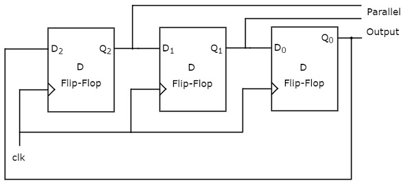
The 3-bit Ring counter contains only a 3-bit SIPO shift register. The output of rightmost D flip-flop is connected to serial input of left most D flip-flop.
Assume, initial status of the D flip-flops from leftmost to rightmost is $\mathrm{Q_{2}Q_{1}Q_{0} \: = \: 001}$. Here, $\mathrm{Q_{2}}$ & $\mathrm{Q_{0}}$ are MSB & LSB respectively. We can understand the working of Ring counter from the following table.
| No of positive edge of Clock | Serial Input = Q0 | Q2(MSB) | Q1 | Q0(LSB) |
|---|---|---|---|---|
| 0 | - | 0 | 0 | 1 |
| 1 | 1 | 1 | 0 | 0 |
| 2 | 0 | 0 | 1 | 0 |
| 3 | 0 | 0 | 0 | 1 |
The initial status of the D flip-flops in the absence of clock signal is $\mathrm{Q_{2}Q_{1}Q_{0} \: = \: 001}$. This status repeats for every three positive edge transitions of clock signal.
Therefore, the following operations take place for every positive edge of clock signal.
Serial input of first D flip-flop gets the previous output of third flip-flop. So, the present output of first D flip-flop is equal to the previous output of third flip-flop.
The previous outputs of first and second D flip-flops are right shifted by one bit. That means, the present outputs of second and third D flip-flops are equal to the previous outputs of first and second D flip-flops.
Johnson Ring Counter
The operation of Johnson Ring counter is similar to that of Ring counter. But, the only difference is that the complemented output of rightmost D flip-flop is given as input of leftmost D flip-flop instead of normal output. Therefore, N bit Johnson Ring counter produces a sequence of states (pattern of zeros and ones) and it repeats for every 2N clock cycles.
Johnson Ring counter is also called as Twisted Ring counter and switch tail Ring counter. The block diagram of 3-bit Johnson Ring counter is shown in the following figure.
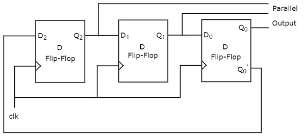
The 3-bit Johnson Ring counter also contains only a 3-bit SIPO shift register. The complemented output of rightmost D flip-flop is connected to serial input of left most D flip-flop.
Assume, initially all the D flip-flops are cleared. So, $\mathrm{Q_{2}Q_{1}Q_{0} \: = \: 000}$. Here, $\mathrm{Q_{2}}$ & $\mathrm{Q_{0}}$ are MSB & LSB respectively. We can understand the working of Johnson Ring counter from the following table.
| No of positive edge of Clock | Serial Input = Q0 | Q2(MSB) | Q1 | Q0(LSB) |
|---|---|---|---|---|
| 0 | - | 0 | 0 | 0 |
| 1 | 1 | 1 | 0 | 0 |
| 2 | 1 | 1 | 1 | 0 |
| 3 | 1 | 1 | 1 | 1 |
| 4 | 0 | 0 | 1 | 1 |
| 5 | 0 | 0 | 0 | 1 |
| 6 | 0 | 0 | 0 | 0 |
The initial status of the D flip-flops in the absence of clock signal is $\mathrm{Q_{2}Q_{1}Q_{0} \: = \: 000}$. This status repeats for every six positive edge transitions of clock signal.
Therefore, the following operations take place for every positive edge of clock signal.
Serial input of first D flip-flop gets the previous complemented output of third flip-flop. So, the present output of first D flip-flop is equal to the previous complemented output of third flip-flop.
The previous outputs of first and second D flip-flops are right shifted by one bit. That means, the present outputs of second and third D flip-flops are equal to the previous outputs of first and second D flip-flops.