- Digital Electronics - Home
- Digital Electronics Basics
- Types of Digital Systems
- Types of Signals
- Logic Levels And Pulse Waveforms
- Digital System Components
- Digital Logic Operations
- Digital Systems Advantages
- Number Systems
- Number Systems
- Binary Numbers Representation
- Binary Arithmetic
- Signed Binary Arithmetic
- Octal Arithmetic
- Hexadecimal Arithmetic
- Complement Arithmetic
- Base Conversions
- Base Conversions
- Binary to Decimal Conversion
- Decimal to Binary Conversion
- Binary to Octal Conversion
- Octal to Binary Conversion
- Octal to Decimal Conversion
- Decimal to Octal Conversion
- Hexadecimal to Binary Conversion
- Binary to Hexadecimal Conversion
- Hexadecimal to Decimal Conversion
- Decimal to Hexadecimal Conversion
- Octal to Hexadecimal Conversion
- Hexadecimal to Octal Conversion
- Binary Codes
- Binary Codes
- 8421 BCD Code
- Excess-3 Code
- Gray Code
- ASCII Codes
- EBCDIC Code
- Code Conversion
- Error Detection & Correction Codes
- Logic Gates
- Logic Gates
- AND Gate
- OR Gate
- NOT Gate
- Universal Gates
- XOR Gate
- XNOR Gate
- CMOS Logic Gate
- OR Gate Using Diode Resistor Logic
- AND Gate vs OR Gate
- Two Level Logic Realization
- Threshold Logic
- Boolean Algebra
- Boolean Algebra
- Laws of Boolean Algebra
- Boolean Functions
- DeMorgan's Theorem
- SOP and POS Form
- POS to Standard POS Form
- Minimization Techniques
- K-Map Minimization
- Three Variable K-Map
- Four Variable K-Map
- Five Variable K-Map
- Six Variable K-Map
- Don't Care Condition
- Quine-McCluskey Method
- Min Terms and Max Terms
- Canonical and Standard Form
- Max Term Representation
- Simplification using Boolean Algebra
- Combinational Logic Circuits
- Digital Combinational Circuits
- Digital Arithmetic Circuits
- Multiplexers
- Multiplexer Design Procedure
- Mux Universal Gate
- 2-Variable Function Using 4:1 Mux
- 3-Variable Function Using 8:1 Mux
- Demultiplexers
- Mux vs Demux
- Parity Bit Generator and Checker
- Comparators
- Encoders
- Keyboard Encoders
- Priority Encoders
- Decoders
- Arithmetic Logic Unit
- 7-Segment LED Display
- Code Converters
- Code Converters
- Binary to Decimal Converter
- Decimal to BCD Converter
- BCD to Decimal Converter
- Binary to Gray Code Converter
- Gray Code to Binary Converter
- BCD to Excess-3 Converter
- Excess-3 to BCD Converter
- Adders
- Half Adders
- Full Adders
- Serial Adders
- Parallel Adders
- Full Adder using Half Adder
- Half Adder vs Full Adder
- Full Adder with NAND Gates
- Half Adder with NAND Gates
- Binary Adder-Subtractor
- Subtractors
- Half Subtractors
- Full Subtractors
- Parallel Subtractors
- Full Subtractor using 2 Half Subtractors
- Half Subtractor using NAND Gates
- Sequential Logic Circuits
- Digital Sequential Circuits
- Clock Signal and Triggering
- Latches
- Shift Registers
- Shift Register Applications
- Binary Registers
- Bidirectional Shift Register
- Counters
- Binary Counters
- Non-binary Counter
- Design of Synchronous Counter
- Synchronous vs Asynchronous Counter
- Finite State Machines
- Algorithmic State Machines
- Flip Flops
- Flip-Flops
- Conversion of Flip-Flops
- D Flip-Flops
- JK Flip-Flops
- T Flip-Flops
- SR Flip-Flops
- Clocked SR Flip-Flop
- Unclocked SR Flip-Flop
- Clocked JK Flip-Flop
- JK to T Flip-Flop
- SR to JK Flip-Flop
- Triggering Methods:Flip-Flop
- Edge-Triggered Flip-Flop
- Master-Slave JK Flip-Flop
- Race-around Condition
- A/D and D/A Converters
- Analog-to-Digital Converter
- Digital-to-Analog Converter
- DAC and ADC ICs
- Realization of Logic Gates
- NOT Gate from NAND Gate
- OR Gate from NAND Gate
- AND Gate from NAND Gate
- NOR Gate from NAND Gate
- XOR Gate from NAND Gate
- XNOR Gate from NAND Gate
- NOT Gate from NOR Gate
- OR Gate from NOR Gate
- AND Gate from NOR Gate
- NAND Gate from NOR Gate
- XOR Gate from NOR Gate
- XNOR Gate from NOR Gate
- NAND/NOR Gate using CMOS
- Full Subtractor using NAND Gate
- AND Gate Using 2:1 MUX
- OR Gate Using 2:1 MUX
- NOT Gate Using 2:1 MUX
- Memory Devices
- Memory Devices
- RAM and ROM
- Cache Memory Design
- Programmable Logic Devices
- Programmable Logic Devices
- Programmable Logic Array
- Programmable Array Logic
- Field Programmable Gate Arrays
- Digital Electronics Families
- Digital Electronics Families
- CPU Architecture
- CPU Architecture
Digital Electronics - Counters
Counter is a sequential circuit. A digital circuit which is used for a counting pulses is known counter. Counter is the widest application of flip-flops. It is a group of flip-flops with a clock signal applied. Counters are of two types.
- Asynchronous or Ripple Counters
- Synchronous Counters
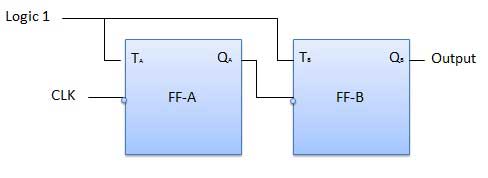
Asynchronous or Ripple Counters
The logic diagram of a 2-bit ripple up counter is shown in figure. The toggle (T) flip-flop are being used. But we can use the JK flip-flop also with J and K connected permanently to logic 1. External clock is applied to the clock input of flip-flop A and QA output is applied to the clock input of the next flip-flop i.e. FF-B.
Logical Diagram
Operation
| Sr.No | Condition | Operation |
|---|---|---|
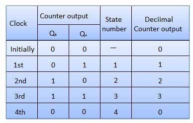
| 1 | Initially let both the FFs be in the reset state | QBQA = 00 initially |
| 2 | After 1st negative clock edge |
As soon as the first negative clock edge is applied, FF-A will toggle and QA will be equal to 1. QA is connected to clock input of FF-B. Since QA has changed from 0 to 1, it is treated as the positive clock edge by FF-B. There is no change in QB because FF-B is a negative edge triggered FF. QBQA = 01 after the first clock pulse. |
| 3 | After 2nd negative clock edge |
On the arrival of second negative clock edge, FF-A toggles again and QA = 0. The change in QA acts as a negative clock edge for FF-B. So it will also toggle, and QB will be 1. QBQA = 10 after the second clock pulse. |
| 4 | After 3rd negative clock edge |
On the arrival of 3rd negative clock edge, FF-A toggles again and QA become 1 from 0. Since this is a positive going change, FF-B does not respond to it and remains inactive. So QB does not change and continues to be equal to 1. QBQA = 11 after the third clock pulse. |
| 5 | After 4th negative clock edge |
On the arrival of 4th negative clock edge, FF-A toggles again and QA becomes 1 from 0. This negative change in QA acts as clock pulse for FF-B. Hence it toggles to change QB from 1 to 0. QBQA = 00 after the fourth clock pulse. |
Truth Table
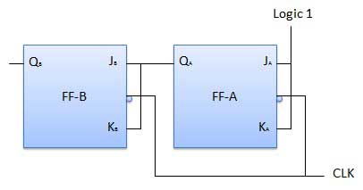
Synchronous Counters
If the "clock" pulses are applied to all the flip-flops in a counter simultaneously, then such a counter is called as synchronous counter.
2-bit Synchronous Up Counter
The JA and KA inputs of FF-A are tied to logic 1. So FF-A will work as a toggle flip-flop. The JB and KB inputs are connected to QA.
Logical Diagram
Operation
| Sr.No | Condition | Operation |
|---|---|---|
| 1 | Initially let both the FFs be in the reset state | QBQA = 00 initially. |
| 2 | After 1st negative clock edge |
As soon as the first negative clock edge is applied, FF-A will toggle and QA will change from 0 to 1. But at the instant of application of negative clock edge, QA , JB = KB = 0. Hence FF-B will not change its state. So QB will remain 0. QBQA = 01 after the first clock pulse. |
| 3 | After 2nd negative clock edge |
On the arrival of second negative clock edge, FF-A toggles again and QA changes from 1 to 0. But at this instant QA was 1. So JB = KB= 1 and FF-B will toggle. Hence QB changes from 0 to 1. QBQA = 10 after the second clock pulse. |
| 4 | After 3rd negative clock edge |
On application of the third falling clock edge, FF-A will toggle from 0 to 1 but there is no change of state for FF-B. QBQA = 11 after the third clock pulse. |
| 5 | After 4th negative clock edge |
On application of the next clock pulse, QA will change from 1 to 0 as QB will also change from 1 to 0. QBQA = 00 after the fourth clock pulse. |
Classification of Counters
Depending on the way in which the counting progresses, the synchronous or asynchronous counters are classified as follows −
- Up Counters
- Down Counters
- Up/Down Counters
UP/DOWN Counter
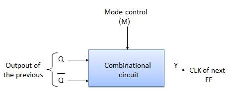
Up counter and down counter is combined together to obtain an UP/DOWN counter. A mode control (M) input is also provided to select either up or down mode. A combinational circuit is required to be designed and used between each pair of flip-flop in order to achieve the up/down operation.
Type of Up/Down Counters
There are two types of up/down counters −
- UP/DOWN Ripple Counters
- UP/DOWN Synchronous Counter
UP/DOWN Ripple Counters
In the UP/DOWN ripple counter all the FFs operate in the toggle mode. So either T flip-flops or JK flip-flops are to be used. The LSB flip-flop receives clock directly. But the clock to every other FF is obtained from (Q = Q bar) output of the previous FF.
- UP counting mode (M=0) − The Q output of the preceding FF is connected to the clock of the next stage if up counting is to be achieved. For this mode, the mode select input M is at logic 0 (M=0).
- DOWN counting mode (M=1) − If M = 1, then the Q bar output of the preceding FF is connected to the next FF. This will operate the counter in the counting mode.
Example
3-bit binary up/down ripple counter.
- 3-bit − hence three FFs are required.
- UP/DOWN − So a mode control input is essential.
- For a ripple up counter, the Q output of preceding FF is connected to the clock input of the next one.
- For a ripple up counter, the Q output of preceding FF is connected to the clock input of the next one.
- For a ripple down counter, the Q bar output of preceding FF is connected to the clock input of the next one.
- Let the selection of Q and Q bar output of the preceding FF be controlled by the mode control input M such that, If M = 0, UP counting. So connect Q to CLK. If M = 1, DOWN counting. So connect Q bar to CLK.
Block Diagram
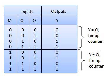
Truth Table
Operation
| Sr.No | Condition | Operation |
|---|---|---|
| 1 | Case 1 − With M = 0 (Up counting mode) |
If M = 0 and M bar = 1, then the AND gates 1 and 3 in fig. will be enabled whereas the AND gates 2 and 4 will be disabled. Hence QA gets connected to the clock input of FF-B and QB gets connected to the clock input of FF-C. These connections are same as those for the normal up counter. Thus with M = 0 the circuit work as an up counter. |
| 2 | Case 2 − With M = 1 (Down counting mode) |
If M = 1, then AND gates 2 and 4 in fig. are enabled whereas the AND gates 1 and 3 are disabled. Hence QA bar gets connected to the clock input of FF-B and QB bar gets connected to the clock input of FF-C. These connections will produce a down counter. Thus with M = 1 the circuit works as a down counter. |
Modulus Counter (MOD-N Counter)
The 2-bit ripple counter is called as MOD-4 counter and 3-bit ripple counter is called as MOD-8 counter. So in general, an n-bit ripple counter is called as modulo-N counter. Where, MOD number = 2n.
Type of Modulus
- 2-bit up or down (MOD-4)
- 3-bit up or down (MOD-8)
- 4-bit up or down (MOD-16)
Application of Counters
- Frequency counters
- Digital clock
- Time measurement
- A to D converter
- Frequency divider circuits
- Digital triangular wave generator.