- Digital Electronics - Home
- Digital Electronics Basics
- Types of Digital Systems
- Types of Signals
- Logic Levels And Pulse Waveforms
- Digital System Components
- Digital Logic Operations
- Digital Systems Advantages
- Number Systems
- Number Systems
- Binary Numbers Representation
- Binary Arithmetic
- Signed Binary Arithmetic
- Octal Arithmetic
- Hexadecimal Arithmetic
- Complement Arithmetic
- Base Conversions
- Base Conversions
- Binary to Decimal Conversion
- Decimal to Binary Conversion
- Binary to Octal Conversion
- Octal to Binary Conversion
- Octal to Decimal Conversion
- Decimal to Octal Conversion
- Hexadecimal to Binary Conversion
- Binary to Hexadecimal Conversion
- Hexadecimal to Decimal Conversion
- Decimal to Hexadecimal Conversion
- Octal to Hexadecimal Conversion
- Hexadecimal to Octal Conversion
- Binary Codes
- Binary Codes
- 8421 BCD Code
- Excess-3 Code
- Gray Code
- ASCII Codes
- EBCDIC Code
- Code Conversion
- Error Detection & Correction Codes
- Logic Gates
- Logic Gates
- AND Gate
- OR Gate
- NOT Gate
- Universal Gates
- XOR Gate
- XNOR Gate
- CMOS Logic Gate
- OR Gate Using Diode Resistor Logic
- AND Gate vs OR Gate
- Two Level Logic Realization
- Threshold Logic
- Boolean Algebra
- Boolean Algebra
- Laws of Boolean Algebra
- Boolean Functions
- DeMorgan's Theorem
- SOP and POS Form
- POS to Standard POS Form
- Minimization Techniques
- K-Map Minimization
- Three Variable K-Map
- Four Variable K-Map
- Five Variable K-Map
- Six Variable K-Map
- Don't Care Condition
- Quine-McCluskey Method
- Min Terms and Max Terms
- Canonical and Standard Form
- Max Term Representation
- Simplification using Boolean Algebra
- Combinational Logic Circuits
- Digital Combinational Circuits
- Digital Arithmetic Circuits
- Multiplexers
- Multiplexer Design Procedure
- Mux Universal Gate
- 2-Variable Function Using 4:1 Mux
- 3-Variable Function Using 8:1 Mux
- Demultiplexers
- Mux vs Demux
- Parity Bit Generator and Checker
- Comparators
- Encoders
- Keyboard Encoders
- Priority Encoders
- Decoders
- Arithmetic Logic Unit
- 7-Segment LED Display
- Code Converters
- Code Converters
- Binary to Decimal Converter
- Decimal to BCD Converter
- BCD to Decimal Converter
- Binary to Gray Code Converter
- Gray Code to Binary Converter
- BCD to Excess-3 Converter
- Excess-3 to BCD Converter
- Adders
- Half Adders
- Full Adders
- Serial Adders
- Parallel Adders
- Full Adder using Half Adder
- Half Adder vs Full Adder
- Full Adder with NAND Gates
- Half Adder with NAND Gates
- Binary Adder-Subtractor
- Subtractors
- Half Subtractors
- Full Subtractors
- Parallel Subtractors
- Full Subtractor using 2 Half Subtractors
- Half Subtractor using NAND Gates
- Sequential Logic Circuits
- Digital Sequential Circuits
- Clock Signal and Triggering
- Latches
- Shift Registers
- Shift Register Applications
- Binary Registers
- Bidirectional Shift Register
- Counters
- Binary Counters
- Non-binary Counter
- Design of Synchronous Counter
- Synchronous vs Asynchronous Counter
- Finite State Machines
- Algorithmic State Machines
- Flip Flops
- Flip-Flops
- Conversion of Flip-Flops
- D Flip-Flops
- JK Flip-Flops
- T Flip-Flops
- SR Flip-Flops
- Clocked SR Flip-Flop
- Unclocked SR Flip-Flop
- Clocked JK Flip-Flop
- JK to T Flip-Flop
- SR to JK Flip-Flop
- Triggering Methods:Flip-Flop
- Edge-Triggered Flip-Flop
- Master-Slave JK Flip-Flop
- Race-around Condition
- A/D and D/A Converters
- Analog-to-Digital Converter
- Digital-to-Analog Converter
- DAC and ADC ICs
- Realization of Logic Gates
- NOT Gate from NAND Gate
- OR Gate from NAND Gate
- AND Gate from NAND Gate
- NOR Gate from NAND Gate
- XOR Gate from NAND Gate
- XNOR Gate from NAND Gate
- NOT Gate from NOR Gate
- OR Gate from NOR Gate
- AND Gate from NOR Gate
- NAND Gate from NOR Gate
- XOR Gate from NOR Gate
- XNOR Gate from NOR Gate
- NAND/NOR Gate using CMOS
- Full Subtractor using NAND Gate
- AND Gate Using 2:1 MUX
- OR Gate Using 2:1 MUX
- NOT Gate Using 2:1 MUX
- Memory Devices
- Memory Devices
- RAM and ROM
- Cache Memory Design
- Programmable Logic Devices
- Programmable Logic Devices
- Programmable Logic Array
- Programmable Array Logic
- Field Programmable Gate Arrays
- Digital Electronics Families
- Digital Electronics Families
- CPU Architecture
- CPU Architecture
Digital Electronics - Decoders
What is a Decoder?
In digital electronics, a combinational logic circuit that converts an N-bit binary input code into M output channels in such a way that only one output channel is activated for each one of the possible combinations of inputs is known as a decoder.
In other words, a combinational logic circuit which converts N input lines into a maximum of 2N output lines is called a decoder.
Therefore, a decoder is a combination logic circuit that is capable of identifying or detecting a particular code. The operation that a decoder performs is referred to as decoding. A general block diagram of a decoder is shown in Figure-1.
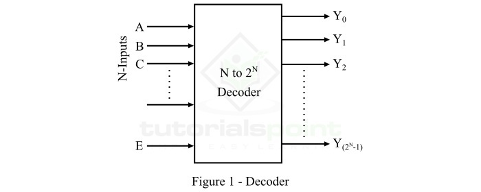
Here, the decoder has N input lines and M (2N) output lines. In a decoder, each of the N input lines can be a 0 or a 1, hence the number of possible input combinations or codes be equal to 2N. For each of these input combinations, only one of the M output lines will be active, and all other output lines will remain inactive.
Types of Decoders
There are several types of decoder present. But, based on the input and output lines present, decoders may classified into the following three types −
- 2 to 4 Decoder
- 3 to 8 Decoder
- 4 to 16 Decoder
Now, let us discuss each type of decoder in detail one by one.
2 to 4 Decoder
The 2 to 4 decoder is one that has 2 input lines and 4 (22) output lines. The functional block diagram of the 2 to 4 decoder is shown in Figure-2.
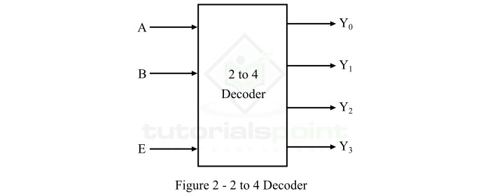
When this decoder is enabled with the help of enable input E, then its one of the four outputs will be active for each combination of inputs. The operation of this 2-line to 4-line decoder can be analyzed with the help of its truth table which is given below.
| Inputs | Outputs | |||||
|---|---|---|---|---|---|---|
| E | A | B | Y3 | Y2 | Y1 | Y0 |
| 0 | X | X | 0 | 0 | 0 | 0 |
| 1 | 0 | 0 | 0 | 0 | 0 | 1 |
| 1 | 0 | 1 | 0 | 0 | 1 | 0 |
| 1 | 1 | 0 | 0 | 1 | 0 | 0 |
| 1 | 1 | 1 | 1 | 0 | 0 | 0 |
Using this truth table, we can derive the Boolean expression for each output as follows −
$$\mathrm{Y_{0} \: = \: E \: \cdot \: \bar{A} \: \cdot \: \bar{B}}$$
$$\mathrm{Y_{1} \: = \: E \: \cdot \: \bar{A} \: \cdot \: B}$$
$$\mathrm{Y_{2} \: = \: E \: \cdot \: A \: \cdot \: \bar{B}}$$
$$\mathrm{Y_{3} \: = \: E \: \cdot \: A \: \cdot \: B}$$
As each output term contains products of input variables that can be implemented with the help of AND gates. Therefore, the logic circuit diagram of the 2 to 4 decoder is shown in Figure-3.
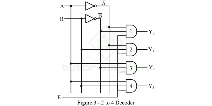
Operation
The operation of logic circuit of the 2 to 4 decoder is described as follows −
- When enable input (E) is inactive, i.e. set to 0, none of the AND gates will function.
- When enable input (E) is made active by setting it to 1, then the circuit works as explained below.
- When A = 0 and B = 0, the AND gate 1 becomes active and produces output Y0.
- When A = 0 and B = 1, the AND gate 2 becomes active and produces output Y1.
- When A = 1 and B = 0, the AND gate 3 becomes active and produces output Y2.
- When A = 1 and B = 1, the AND gate 4 becomes active and produces output Y3.
3 to 8 Decoder
The 3 to 8 decoder is one that has 3 input lines and 8 (23) output lines. The functional block diagram of the 3 to 8 decoder is shown in Figure-4.
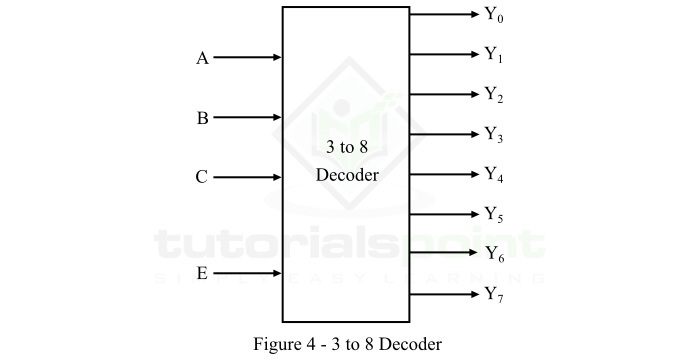
When this decoder is enabled with the help of enable input E, then it's one of the eight outputs will be active for each combination of inputs. The operation of this 3-line to 8-line decoder can be analyzed with the help of its function table which is given below.
| Inputs | Outputs | ||||||||||
|---|---|---|---|---|---|---|---|---|---|---|---|
| E | A | B | C | Y7 | Y6 | Y5 | Y4 | Y3 | Y2 | Y1 | Y0 |
| 0 | X | X | X | 0 | 0 | 0 | 0 | 0 | 0 | 0 | 0 |
| 1 | 0 | 0 | 0 | 0 | 0 | 0 | 0 | 0 | 0 | 0 | 1 |
| 1 | 0 | 0 | 1 | 0 | 0 | 0 | 0 | 0 | 0 | 1 | 0 |
| 1 | 0 | 1 | 0 | 0 | 0 | 0 | 0 | 0 | 1 | 0 | 0 |
| 1 | 0 | 1 | 1 | 0 | 0 | 0 | 0 | 1 | 0 | 0 | 0 |
| 1 | 1 | 0 | 0 | 0 | 0 | 0 | 1 | 0 | 0 | 0 | 0 |
| 1 | 1 | 0 | 1 | 0 | 0 | 1 | 0 | 0 | 0 | 0 | 0 |
| 1 | 1 | 1 | 0 | 0 | 1 | 0 | 0 | 0 | 0 | 0 | 0 |
| 1 | 1 | 1 | 1 | 1 | 0 | 0 | 0 | 0 | 0 | 0 | 0 |
Using this function table, we can derive the Boolean expression for each output as follows −
$$\mathrm{Y_{0} \: = \: E \: \bar{A} \: \bar{B} \: \bar{C}}$$
$$\mathrm{Y_{1} \: = \: E \: \bar{A} \: \bar{B} \: C}$$
$$\mathrm{Y_{2} \: = \: E \: \bar{A} \: B \: \bar{C}}$$
$$\mathrm{Y_{3} \: = \: E \: \bar{A} \: B \: C}$$
$$\mathrm{Y_{4} \: = \: E \: A \: \bar{B} \: \bar{C}}$$
$$\mathrm{Y_{5} \: = \: E \: A \: \bar{B} \: C}$$
$$\mathrm{Y_{6} \: = \: E \: A \: B \: \bar{C}}$$
$$\mathrm{Y_{7} \: = \: E \: A \: B \: C}$$
As we can see, each output term contains products of input variables, hence they can be implemented with the help of AND gates. Therefore, the logic circuit diagram of the 3 to 8 decoder is shown in Figure-5.
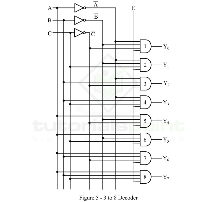
Operation
The operation of logic circuit of the 3 to 8 decoder is described as follows −
- When enable input (E) is inactive, i.e. set to 0, none of the AND gates will function.
- When enable input (E) is made active by setting it to 1, then the circuit works as described below.
- When A = 0, B = 0, and C = 0, the AND gate 1 becomes active and produces output Y0.
- When A = 0, B = 0, and C = 1, the AND gate 2 becomes active and produces output Y1.
- When A = 0, B = 1, and C = 0, the AND gate 3 becomes active and produces output Y2.
- When A = 0, B = 1, and C = 1, the AND gate 4 becomes active and produces output Y3.
- When A = 1, B = 0, and C = 0, the AND gate 5 becomes active and produces output Y4.
- When A = 1, B = 0, and C = 1, the AND gate 6 becomes active and produces output Y5.
- When A = 1, B = 1, and C = 0, the AND gate 7 becomes active and produces output Y6.
- When A = 1, B = 1, and C = 1, the AND gate 8 becomes active and produces output Y7.
4 to 16 Decoder
The 4 to 16 decoder is the type of decoder which has 4 input lines and 16 (214) output lines. The functional block diagram of the 4 to 16 decoder is shown in Figure-6.
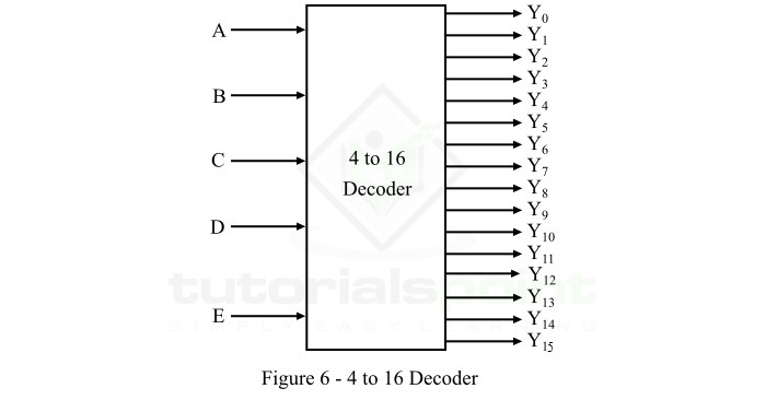
When this decoder is enabled with the help of enable input E, it's one of the sixteen outputs will be active for each combination of inputs. The operation of the 4-line to 16-line decoder can be analyzed with the help of its function table which is given below.
| Inputs | Output | ||||
|---|---|---|---|---|---|
| E | A | B | C | D | |
| 0 | X | X | X | X | 0 |
| 1 | 0 | 0 | 0 | 0 | Y0 |
| 1 | 0 | 0 | 0 | 1 | Y1 |
| 1 | 0 | 0 | 1 | 0 | Y2 |
| 1 | 0 | 0 | 1 | 1 | Y3 |
| 1 | 0 | 1 | 0 | 0 | Y4 |
| 1 | 0 | 1 | 0 | 1 | Y5 |
| 1 | 0 | 1 | 1 | 0 | Y6 |
| 1 | 0 | 1 | 1 | 1 | Y7 |
| 1 | 1 | 0 | 0 | 0 | Y8 |
| 1 | 1 | 0 | 0 | 1 | Y9 |
| 1 | 1 | 0 | 1 | 0 | Y10 |
| 1 | 1 | 0 | 1 | 1 | Y11 |
| 1 | 1 | 1 | 0 | 0 | Y12 |
| 1 | 1 | 1 | 0 | 1 | Y13 |
| 1 | 1 | 1 | 1 | 0 | Y14 |
| 1 | 1 | 1 | 1 | 1 | Y15 |
From this function table, we can directly write the Boolean expression for each output as follows −
$$\mathrm{Y_{0} \: = \: E \: \bar{A} \: \bar{B} \: \bar{C} \: \bar{D}}$$
$$\mathrm{Y_{1} \: = \: E \: \bar{A} \: \bar{B} \: \bar{C} \: D}$$
$$\mathrm{Y_{2} \: = \: E \: \bar{A} \: \bar{B} \: C \: \bar{D}}$$
$$\mathrm{Y_{3} \: = \: E \: \bar{A} \: \bar{B} \: C \: D}$$
$$\mathrm{Y_{4} \: = \: E \: \bar{A} \: B \: \bar{C} \: \bar{D}}$$
$$\mathrm{Y_{5} \: = \: E \: \bar{A} \: B \: \bar{C} \: D}$$
$$\mathrm{Y_{6} \: = \: E \: \bar{A} \: B \: C \: \bar{D}}$$
$$\mathrm{Y_{7} \: = \: E \: \bar{A} \: B \: C \: D}$$
$$\mathrm{Y_{8} \: = \: E \: A \: \bar{B} \: \bar{C} \: \bar{D}}$$
$$\mathrm{Y_{9} \: = \: E \: A \: \bar{B} \: \bar{C} \: D}$$
$$\mathrm{Y_{10} \: = \: E \: A \: \bar{B} \: C \: \bar{D}}$$
$$\mathrm{Y_{11} \: = \: E \: A \: \bar{B} \: C \: D}$$
$$\mathrm{Y_{12} \: = \: E \: A \: B \: \bar{C} \: \bar{D}}$$
$$\mathrm{Y_{13} \: = \: E \: A \: B \: \bar{C} \: D}$$
$$\mathrm{Y_{14} \: = \: E \: A \: B \: C \: \bar{D}}$$
$$\mathrm{Y_{15} \: = \: E \: A \: B \: C \: D}$$
We can implement these output expression in the same way as we done for the 2 to 4 decoder and 3 to 8 decoder.
Now, let us discuss the applications of decoders.
Applications of Decoders
Decoders are used in the cases where an output or a collection of outputs is to be activated only on the occurrence of a particular combination of input codes. Some important applications of decoders are listed below −
- Decoders are used for code conversions.
- Decoders are extensively used in memory systems of computers.
- Decoders are also used for de-multiplexing or data distribution.
- Decoders are also used in data routing applications where very short propagation delay is required.
- Decoder may also be used for timing or sequencing purposes.
- Decoders are also utilized to turn on and off digital devices at a specific time.
This is all about decoder and its applications in digital electronic systems.