- Digital Electronics - Home
- Digital Electronics Basics
- Types of Digital Systems
- Types of Signals
- Logic Levels And Pulse Waveforms
- Digital System Components
- Digital Logic Operations
- Digital Systems Advantages
- Number Systems
- Number Systems
- Binary Numbers Representation
- Binary Arithmetic
- Signed Binary Arithmetic
- Octal Arithmetic
- Hexadecimal Arithmetic
- Complement Arithmetic
- Base Conversions
- Base Conversions
- Binary to Decimal Conversion
- Decimal to Binary Conversion
- Binary to Octal Conversion
- Octal to Binary Conversion
- Octal to Decimal Conversion
- Decimal to Octal Conversion
- Hexadecimal to Binary Conversion
- Binary to Hexadecimal Conversion
- Hexadecimal to Decimal Conversion
- Decimal to Hexadecimal Conversion
- Octal to Hexadecimal Conversion
- Hexadecimal to Octal Conversion
- Binary Codes
- Binary Codes
- 8421 BCD Code
- Excess-3 Code
- Gray Code
- ASCII Codes
- EBCDIC Code
- Code Conversion
- Error Detection & Correction Codes
- Logic Gates
- Logic Gates
- AND Gate
- OR Gate
- NOT Gate
- Universal Gates
- XOR Gate
- XNOR Gate
- CMOS Logic Gate
- OR Gate Using Diode Resistor Logic
- AND Gate vs OR Gate
- Two Level Logic Realization
- Threshold Logic
- Boolean Algebra
- Boolean Algebra
- Laws of Boolean Algebra
- Boolean Functions
- DeMorgan's Theorem
- SOP and POS Form
- POS to Standard POS Form
- Minimization Techniques
- K-Map Minimization
- Three Variable K-Map
- Four Variable K-Map
- Five Variable K-Map
- Six Variable K-Map
- Don't Care Condition
- Quine-McCluskey Method
- Min Terms and Max Terms
- Canonical and Standard Form
- Max Term Representation
- Simplification using Boolean Algebra
- Combinational Logic Circuits
- Digital Combinational Circuits
- Digital Arithmetic Circuits
- Multiplexers
- Multiplexer Design Procedure
- Mux Universal Gate
- 2-Variable Function Using 4:1 Mux
- 3-Variable Function Using 8:1 Mux
- Demultiplexers
- Mux vs Demux
- Parity Bit Generator and Checker
- Comparators
- Encoders
- Keyboard Encoders
- Priority Encoders
- Decoders
- Arithmetic Logic Unit
- 7-Segment LED Display
- Code Converters
- Code Converters
- Binary to Decimal Converter
- Decimal to BCD Converter
- BCD to Decimal Converter
- Binary to Gray Code Converter
- Gray Code to Binary Converter
- BCD to Excess-3 Converter
- Excess-3 to BCD Converter
- Adders
- Half Adders
- Full Adders
- Serial Adders
- Parallel Adders
- Full Adder using Half Adder
- Half Adder vs Full Adder
- Full Adder with NAND Gates
- Half Adder with NAND Gates
- Binary Adder-Subtractor
- Subtractors
- Half Subtractors
- Full Subtractors
- Parallel Subtractors
- Full Subtractor using 2 Half Subtractors
- Half Subtractor using NAND Gates
- Sequential Logic Circuits
- Digital Sequential Circuits
- Clock Signal and Triggering
- Latches
- Shift Registers
- Shift Register Applications
- Binary Registers
- Bidirectional Shift Register
- Counters
- Binary Counters
- Non-binary Counter
- Design of Synchronous Counter
- Synchronous vs Asynchronous Counter
- Finite State Machines
- Algorithmic State Machines
- Flip Flops
- Flip-Flops
- Conversion of Flip-Flops
- D Flip-Flops
- JK Flip-Flops
- T Flip-Flops
- SR Flip-Flops
- Clocked SR Flip-Flop
- Unclocked SR Flip-Flop
- Clocked JK Flip-Flop
- JK to T Flip-Flop
- SR to JK Flip-Flop
- Triggering Methods:Flip-Flop
- Edge-Triggered Flip-Flop
- Master-Slave JK Flip-Flop
- Race-around Condition
- A/D and D/A Converters
- Analog-to-Digital Converter
- Digital-to-Analog Converter
- DAC and ADC ICs
- Realization of Logic Gates
- NOT Gate from NAND Gate
- OR Gate from NAND Gate
- AND Gate from NAND Gate
- NOR Gate from NAND Gate
- XOR Gate from NAND Gate
- XNOR Gate from NAND Gate
- NOT Gate from NOR Gate
- OR Gate from NOR Gate
- AND Gate from NOR Gate
- NAND Gate from NOR Gate
- XOR Gate from NOR Gate
- XNOR Gate from NOR Gate
- NAND/NOR Gate using CMOS
- Full Subtractor using NAND Gate
- AND Gate Using 2:1 MUX
- OR Gate Using 2:1 MUX
- NOT Gate Using 2:1 MUX
- Memory Devices
- Memory Devices
- RAM and ROM
- Cache Memory Design
- Programmable Logic Devices
- Programmable Logic Devices
- Programmable Logic Array
- Programmable Array Logic
- Field Programmable Gate Arrays
- Digital Electronics Families
- Digital Electronics Families
- CPU Architecture
- CPU Architecture
NOT Gate Using 2:1 MUX in Digital Electronics
What is a Multiplexer?
In digital electronics, a multiplexer or MUX is a combinational logic circuit which accepts several data inputs and allows only one of them at a time to flow through the output line. Multiplexer (MUX) is also known as data selector because it selects one from many.
A multiplexer consists of 2n data input lines, n select lines, and 1 output line. Since, it converts 2n input lines into 1 output line. Therefore, it is also called many-to-one device.
Depending upon the number of input lines, there are several types of multiplexer present such as 2:1 MUX, 4:1 MUX, 8:1 MUX, and so on.
Since, this chapter is meant for explaining the implementation of a NOT gate by using a 2:1 MUX. So let us discuss a 2:1 MUX in detail.
2:1 Multiplexer (MUX)
The logic block diagram of a 2:1 multiplexer is shown in Figure-1.
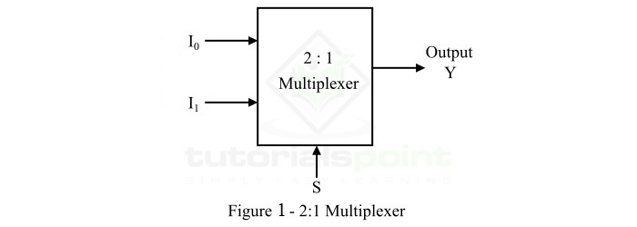
A 2:1 MUX consists of 2 (21) data input lines designated by I0 and I1, 1 select line designated by S and 1 output line Y. The logic level either 0 or 1 applied to the select line S determines which input data will pass through the output line of the multiplexer.
Truth Table of 2:1 Multiplexer
The operation of the 2:1 MUX can be analyzed with the help of its truth table shown below.
| Select Line (S) | Output (Y) |
|---|---|
| 0 | I0 |
| 1 | I1 |
From this truth table, we can conclude that,
- If select line S is connected to logic level 0, the data input connected to I0 will pass through the output line Y.
- If select line S is connected to logic level 1, the data input connected to I1 will pass through the output line Y.
Now, let us discuss about the NOT gate.
What is a NOT Gate?
The NOT Gate is a basic logic gate that used in digital electronic circuits. The NOT gate has a single input and a single output. The output of the NOT gate is the logical inversion of its input. Hence, it is also called an inverter.
The standard logic symbol of the NOT gate has a triangle pointing to the right with a circle at its right end as shown in Figure-2. The circle at right corner is referred to as an inversion bubble.

The NOT gate produces an output which is the complement or inversion of its input. For example, if we give a logic 0 at its input, it will provide a logic 1 at output. Similarly, when we give a logic 1 at input, it produces a logic 0 at output.
Truth Table of NOT Gate
The operation of the NOT gate for all possible inputs can be analyzed with the help of its truth table which is given below.
| Input (A) | Output (Y = A') |
|---|---|
| 0 | 1 |
| 1 | 0 |
From this truth table, we may derive the output equation of the NOT gate, i.e.
$$\mathrm{Y\: = \: \bar{A} \: = \: A'}$$
Hence, it is clear that the NOT gate produces an output which is opposite of the applied input.
Now, we can discuss the realization of a NOT gate using a 2:1 MUX as we have enough knowledge of a 2:1 multiplexer and NOT gate required to do this.
NOT Gate by using 2:1 MUX
The functional block diagram of a 2:1 multiplexer equivalent to the NOT gate is shown in Figure-3.
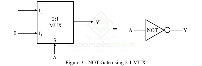
There are two possible inputs, i.e. 0 and 1. We have applied 1 to the input line I0 and 0 to the input line I1. The input variable of the NOT gate is applied to the select line S of the MUX.
The operation of the 2:1 MUX as the NOT gate can be described as follows
- When the input to the select line is A = 0, then the multiplexer will transmit the 1 applied at the input line I0 to the output line.
- When the input to the select line is A = 1, then the multiplexer will transmit the 0 applied at the input line I1 to the output line.
Truth Table of 2:1 MUX Working NOT Gate
The truth table of the 2:1 MUX working as a NOT gate is given as follows,
| S = A | Output (Y) |
|---|---|
| 0 | 1 |
| 1 | 0 |
Hence, the output expression of the NOT gate using 2:1 MUX will be,
$$\mathrm{Y\:=\:\bar{A}\cdot 1 \: + \: A\cdot 0 \: = \: \bar{A}}$$
In this way, we can implement the NOT gate operation by using a 2:1 multiplexer.