- Digital Electronics - Home
- Digital Electronics Basics
- Types of Digital Systems
- Types of Signals
- Logic Levels And Pulse Waveforms
- Digital System Components
- Digital Logic Operations
- Digital Systems Advantages
- Number Systems
- Number Systems
- Binary Numbers Representation
- Binary Arithmetic
- Signed Binary Arithmetic
- Octal Arithmetic
- Hexadecimal Arithmetic
- Complement Arithmetic
- Base Conversions
- Base Conversions
- Binary to Decimal Conversion
- Decimal to Binary Conversion
- Binary to Octal Conversion
- Octal to Binary Conversion
- Octal to Decimal Conversion
- Decimal to Octal Conversion
- Hexadecimal to Binary Conversion
- Binary to Hexadecimal Conversion
- Hexadecimal to Decimal Conversion
- Decimal to Hexadecimal Conversion
- Octal to Hexadecimal Conversion
- Hexadecimal to Octal Conversion
- Binary Codes
- Binary Codes
- 8421 BCD Code
- Excess-3 Code
- Gray Code
- ASCII Codes
- EBCDIC Code
- Code Conversion
- Error Detection & Correction Codes
- Logic Gates
- Logic Gates
- AND Gate
- OR Gate
- NOT Gate
- Universal Gates
- XOR Gate
- XNOR Gate
- CMOS Logic Gate
- OR Gate Using Diode Resistor Logic
- AND Gate vs OR Gate
- Two Level Logic Realization
- Threshold Logic
- Boolean Algebra
- Boolean Algebra
- Laws of Boolean Algebra
- Boolean Functions
- DeMorgan's Theorem
- SOP and POS Form
- POS to Standard POS Form
- Minimization Techniques
- K-Map Minimization
- Three Variable K-Map
- Four Variable K-Map
- Five Variable K-Map
- Six Variable K-Map
- Don't Care Condition
- Quine-McCluskey Method
- Min Terms and Max Terms
- Canonical and Standard Form
- Max Term Representation
- Simplification using Boolean Algebra
- Combinational Logic Circuits
- Digital Combinational Circuits
- Digital Arithmetic Circuits
- Multiplexers
- Multiplexer Design Procedure
- Mux Universal Gate
- 2-Variable Function Using 4:1 Mux
- 3-Variable Function Using 8:1 Mux
- Demultiplexers
- Mux vs Demux
- Parity Bit Generator and Checker
- Comparators
- Encoders
- Keyboard Encoders
- Priority Encoders
- Decoders
- Arithmetic Logic Unit
- 7-Segment LED Display
- Code Converters
- Code Converters
- Binary to Decimal Converter
- Decimal to BCD Converter
- BCD to Decimal Converter
- Binary to Gray Code Converter
- Gray Code to Binary Converter
- BCD to Excess-3 Converter
- Excess-3 to BCD Converter
- Adders
- Half Adders
- Full Adders
- Serial Adders
- Parallel Adders
- Full Adder using Half Adder
- Half Adder vs Full Adder
- Full Adder with NAND Gates
- Half Adder with NAND Gates
- Binary Adder-Subtractor
- Subtractors
- Half Subtractors
- Full Subtractors
- Parallel Subtractors
- Full Subtractor using 2 Half Subtractors
- Half Subtractor using NAND Gates
- Sequential Logic Circuits
- Digital Sequential Circuits
- Clock Signal and Triggering
- Latches
- Shift Registers
- Shift Register Applications
- Binary Registers
- Bidirectional Shift Register
- Counters
- Binary Counters
- Non-binary Counter
- Design of Synchronous Counter
- Synchronous vs Asynchronous Counter
- Finite State Machines
- Algorithmic State Machines
- Flip Flops
- Flip-Flops
- Conversion of Flip-Flops
- D Flip-Flops
- JK Flip-Flops
- T Flip-Flops
- SR Flip-Flops
- Clocked SR Flip-Flop
- Unclocked SR Flip-Flop
- Clocked JK Flip-Flop
- JK to T Flip-Flop
- SR to JK Flip-Flop
- Triggering Methods:Flip-Flop
- Edge-Triggered Flip-Flop
- Master-Slave JK Flip-Flop
- Race-around Condition
- A/D and D/A Converters
- Analog-to-Digital Converter
- Digital-to-Analog Converter
- DAC and ADC ICs
- Realization of Logic Gates
- NOT Gate from NAND Gate
- OR Gate from NAND Gate
- AND Gate from NAND Gate
- NOR Gate from NAND Gate
- XOR Gate from NAND Gate
- XNOR Gate from NAND Gate
- NOT Gate from NOR Gate
- OR Gate from NOR Gate
- AND Gate from NOR Gate
- NAND Gate from NOR Gate
- XOR Gate from NOR Gate
- XNOR Gate from NOR Gate
- NAND/NOR Gate using CMOS
- Full Subtractor using NAND Gate
- AND Gate Using 2:1 MUX
- OR Gate Using 2:1 MUX
- NOT Gate Using 2:1 MUX
- Memory Devices
- Memory Devices
- RAM and ROM
- Cache Memory Design
- Programmable Logic Devices
- Programmable Logic Devices
- Programmable Logic Array
- Programmable Array Logic
- Field Programmable Gate Arrays
- Digital Electronics Families
- Digital Electronics Families
- CPU Architecture
- CPU Architecture
Digital to Analog Converter
A Digital to Analog Converter (DAC) converts a digital input signal into an analog output signal. The digital signal is represented with a binary code, which is a combination of bits 0 and 1 while the analog signal is a continuous time function.
This chapter deals with Digital to Analog Converters in detail. The block diagram of DAC is shown in the following figure −
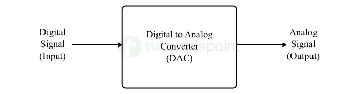
A Digital to Analog Converter (DAC) consists of a number of binary inputs and a single output. In general, the number of binary inputs of a DAC will be a power of two.
Types of Digital to Analog Converters
Depending on the construction and structure, there are two types of digital to analog converters, they are −
- Weighted Resistor DAC
- R-2R Ladder DAC
The following sections discuss about these two types of DACs in detail.
Weighted Resistor DAC
A weighted resistor DAC produces an analog output, which is almost equal to the digital (binary) input by using binary weighted resistors in the inverting adder circuit. In short, a binary weighted resistor DAC is called as weighted resistor DAC.
The circuit diagram of a 3-bit binary weighted resistor DAC is shown in the following figure −
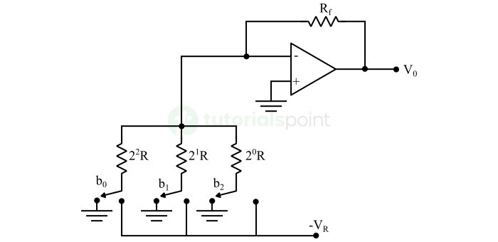
Recall that the bits of a binary number can have only one of the two values. i.e., either 0 or 1. Let the 3-bit binary input is b2b1b0. Here, the bits b2 and b0 denote the Most Significant Bit (MSB) and Least Significant Bit (LSB) respectively.
The digital switches shown in the above figure will be connected to ground, when the corresponding input bits are equal to '0'. Similarly, the digital switches shown in the above figure will be connected to the negative reference voltage, VR when the corresponding input bits are equal to '1'.
In the above circuit, the non-inverting input terminal of an op-amp is connected to ground. That means zero volts is applied at the non-inverting input terminal of op-amp.
According to the virtual short concept, the voltage at the inverting input terminal of op-amp is same as that of the voltage present at its non-inverting input terminal. So, the voltage at the inverting input terminals node will be zero volts.
The nodal equation at the inverting input terminals node is −
$$\mathrm{\frac{0 \: + \: V_{R}b_{2}}{2^{0}R} \: + \: \frac{0 \: + \: V_{R}b_{1}}{2^{1}R} \: + \: \frac{0 \: + \: V_{R}b_{0}}{2^{2}R} \: + \: \frac{0 \: - \: V_{0}}{R_{f}} \: = \: 0}$$
$$\mathrm{\Rightarrow \: \frac{V_{0}}{R_{f}} \: = \: \frac{V_{R}b_{2}}{2^{0}R} \: + \: \frac{V_{R}b_{1}}{2^{1}R} \: + \: \frac{V_{R}b_{0}}{2^{2}R}}$$
$$\mathrm{\Rightarrow \: V_{0} \: = \: \frac{V_{R}R_{f}}{R}(\frac{b_{2}}{2^{0}} \: + \: \frac{b_{1}}{2^{1}} \: + \: \frac{b_{0}}{2^{2}})}$$
Substituting, R = 2Rf in the above equation,
$$\mathrm{V_{0} \: = \: \frac{V_{R}R_{f}}{2R_{f}}(\frac{b_{2}}{2^{0}} \: + \: \frac{b_{1}}{2^{1}} \: + \: \frac{b_{0}}{2^{2}})}$$
$$\mathrm{\therefore \: V_{0} \: = \: \frac{V_{R}}{2}(\frac{b_{2}}{2^{0}} \: + \: \frac{b_{1}}{2^{1}} \: + \: \frac{b_{0}}{2^{2}})}$$
The above equation represents the output voltage equation of a 3-bit binary weighted resistor DAC. Since the number of bits are three in the binary (digital) input, we will get seven possible values of output voltage by varying the binary input from 000 to 111 for a fixed reference voltage, VR.
We can write the generalized output voltage equation of an N-bit binary weighted resistor DAC as shown below based on the output voltage equation of a 3-bit binary weighted resistor DAC.
$$\mathrm{\therefore \: V_{0} \: = \: \frac{V_{R}}{2}(\frac{b_{N-1}}{2^{0}} \: + \: \frac{b_{N-2}}{2^{1}} \: + \dotso \: + \: \frac{b_{0}}{2^{N-1}})}$$
Disadvantages of Weighted Resistor DAC
The disadvantages of the binary weighted resistor DAC are as follows −
- The difference between the resistance values corresponding to LSB & MSB will increase as the number of bits present in the digital input increases.
- It is difficult to design more accurate resistors as the number of bits present in the digital input increases.
R-2R Ladder DAC
The R-2R Ladder DAC overcomes the disadvantages of a binary weighted resistor DAC. As the name suggests, R-2R Ladder DAC produces an analog output, which is almost equal to the digital (binary) input by using a R-2R ladder network in the inverting adder circuit.
The circuit diagram of a 3-bit R-2R Ladder DAC is shown in the following figure −
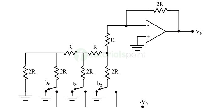
Recall that the bits of a binary number can have only one of the two values. i.e., either 0 or 1. Let the 3-bit binary input is b2b1b0. Here, the bits b2 and b0 denote the Most Significant Bit (MSB) and Least Significant Bit (LSB) respectively.
The digital switches shown in the above figure will be connected to ground, when the corresponding input bits are equal to '0'. Similarly, the digital switches shown in above figure will be connected to the negative reference voltage, VR when the corresponding input bits are equal to '1'.
It is difficult to get the generalized output voltage equation of a R-2R Ladder DAC. But we can find the analog output voltage values of R-2R Ladder DAC for individual binary input combinations easily.
Advantages of R-2R Ladder DAC
The advantages of a R-2R Ladder DAC are as follows −
- R-2R Ladder DAC contains only two values of resistor: R and 2R. So, it is easy to select and design more accurate resistors.
- If a greater number of bits are present in the digital input, then we have to include required number of R-2R sections additionally.
Due to the above advantages, R-2R Ladder DAC is preferable over binary weighted resistor DAC.
Important Parameters of DACs
The following are some key parameters and factors that we must consider while selecting a digital to analog converter for a specific application −
Resolution
The number of discrete output levels that a digital to analog converter can produce is known as its resolution. To obtain a smoother and accurate analog output signal, the resolution of the digital to analog converter must be significantly high. The resolution of a DAC is typically measured in bits.
Let us understand the importance of resolution of DAC. Consider a DAC that can handle 8-bits, it can represent 28 = 256 discrete output values. On the other hand, if a DAC can handle 16-bits, then it is able to represent 216 = 65536 discrete output values. Hence, the DAC with 16-bits can provide a smoother and more accurate representation of the digital signal in analog format as compared to that the 8-bit DAC can do.
Accuracy
The accuracy of a digital to analog converter is the measure of how closer is the output analog signal to the input digital signal. The high accuracy of DAC is an essential factor to produce a highly precise analog output signal.
Power Consumption
This factor provides information about the power consumed by the digital to analog converter during its operation. Ideally, a digital to analog converter must be power efficient, so that it can extend the battery life and minimize the operational cost.
Operating Speed
The operating speed of a digital to analog converter represents the rate at which the DAC converts a digital signal into analog signal. Typically, the speed of a DAC is measured in samples per second (S/s) or megahertz (MHz).
The operating speed of the digital to analog converter also determines the maximum frequency of the analog output signal that the DAC can generate accurately.
It is essential that a digital to analog converter used in applications like real-time signal processing, generation of fast waveforms, high-speed communication, etc. must have a significantly high-speed.
Noise Performance
The noise performance of a digital to analog converter represents the amount of noise that can be introduced in the output signal during the conversion process. The unwanted noise can affect the signal-to-noise ratio and hence the signal quality. Therefore, we should minimize the noise as much as possible to obtain a high-quality output analog signal.
Applications of Digital to Analog Converters
Digital to analog converters are widely used in a variety of applications in the field of digital electronics. The main function of a digital to analog converter is to convert a digital signal into analog format.
The following are some common devices and systems in which the digital to analog converters are used −
- Audio amplifiers and playback systems
- Video encoder systems
- Data acquisition systems
- Calibration of testing and measuring instruments
- Motor control circuits
- Digital signal processors
- Telecommunication systems, etc.
Conclusion
Digital to analog converters are used in the field of electronics to provide an interface between digital input and analog output. In this chapter, we explained in detail about the types and applications of analog to digital converters.