- Digital Electronics - Home
- Digital Electronics Basics
- Types of Digital Systems
- Types of Signals
- Logic Levels And Pulse Waveforms
- Digital System Components
- Digital Logic Operations
- Digital Systems Advantages
- Number Systems
- Number Systems
- Binary Numbers Representation
- Binary Arithmetic
- Signed Binary Arithmetic
- Octal Arithmetic
- Hexadecimal Arithmetic
- Complement Arithmetic
- Base Conversions
- Base Conversions
- Binary to Decimal Conversion
- Decimal to Binary Conversion
- Binary to Octal Conversion
- Octal to Binary Conversion
- Octal to Decimal Conversion
- Decimal to Octal Conversion
- Hexadecimal to Binary Conversion
- Binary to Hexadecimal Conversion
- Hexadecimal to Decimal Conversion
- Decimal to Hexadecimal Conversion
- Octal to Hexadecimal Conversion
- Hexadecimal to Octal Conversion
- Binary Codes
- Binary Codes
- 8421 BCD Code
- Excess-3 Code
- Gray Code
- ASCII Codes
- EBCDIC Code
- Code Conversion
- Error Detection & Correction Codes
- Logic Gates
- Logic Gates
- AND Gate
- OR Gate
- NOT Gate
- Universal Gates
- XOR Gate
- XNOR Gate
- CMOS Logic Gate
- OR Gate Using Diode Resistor Logic
- AND Gate vs OR Gate
- Two Level Logic Realization
- Threshold Logic
- Boolean Algebra
- Boolean Algebra
- Laws of Boolean Algebra
- Boolean Functions
- DeMorgan's Theorem
- SOP and POS Form
- POS to Standard POS Form
- Minimization Techniques
- K-Map Minimization
- Three Variable K-Map
- Four Variable K-Map
- Five Variable K-Map
- Six Variable K-Map
- Don't Care Condition
- Quine-McCluskey Method
- Min Terms and Max Terms
- Canonical and Standard Form
- Max Term Representation
- Simplification using Boolean Algebra
- Combinational Logic Circuits
- Digital Combinational Circuits
- Digital Arithmetic Circuits
- Multiplexers
- Multiplexer Design Procedure
- Mux Universal Gate
- 2-Variable Function Using 4:1 Mux
- 3-Variable Function Using 8:1 Mux
- Demultiplexers
- Mux vs Demux
- Parity Bit Generator and Checker
- Comparators
- Encoders
- Keyboard Encoders
- Priority Encoders
- Decoders
- Arithmetic Logic Unit
- 7-Segment LED Display
- Code Converters
- Code Converters
- Binary to Decimal Converter
- Decimal to BCD Converter
- BCD to Decimal Converter
- Binary to Gray Code Converter
- Gray Code to Binary Converter
- BCD to Excess-3 Converter
- Excess-3 to BCD Converter
- Adders
- Half Adders
- Full Adders
- Serial Adders
- Parallel Adders
- Full Adder using Half Adder
- Half Adder vs Full Adder
- Full Adder with NAND Gates
- Half Adder with NAND Gates
- Binary Adder-Subtractor
- Subtractors
- Half Subtractors
- Full Subtractors
- Parallel Subtractors
- Full Subtractor using 2 Half Subtractors
- Half Subtractor using NAND Gates
- Sequential Logic Circuits
- Digital Sequential Circuits
- Clock Signal and Triggering
- Latches
- Shift Registers
- Shift Register Applications
- Binary Registers
- Bidirectional Shift Register
- Counters
- Binary Counters
- Non-binary Counter
- Design of Synchronous Counter
- Synchronous vs Asynchronous Counter
- Finite State Machines
- Algorithmic State Machines
- Flip Flops
- Flip-Flops
- Conversion of Flip-Flops
- D Flip-Flops
- JK Flip-Flops
- T Flip-Flops
- SR Flip-Flops
- Clocked SR Flip-Flop
- Unclocked SR Flip-Flop
- Clocked JK Flip-Flop
- JK to T Flip-Flop
- SR to JK Flip-Flop
- Triggering Methods:Flip-Flop
- Edge-Triggered Flip-Flop
- Master-Slave JK Flip-Flop
- Race-around Condition
- A/D and D/A Converters
- Analog-to-Digital Converter
- Digital-to-Analog Converter
- DAC and ADC ICs
- Realization of Logic Gates
- NOT Gate from NAND Gate
- OR Gate from NAND Gate
- AND Gate from NAND Gate
- NOR Gate from NAND Gate
- XOR Gate from NAND Gate
- XNOR Gate from NAND Gate
- NOT Gate from NOR Gate
- OR Gate from NOR Gate
- AND Gate from NOR Gate
- NAND Gate from NOR Gate
- XOR Gate from NOR Gate
- XNOR Gate from NOR Gate
- NAND/NOR Gate using CMOS
- Full Subtractor using NAND Gate
- AND Gate Using 2:1 MUX
- OR Gate Using 2:1 MUX
- NOT Gate Using 2:1 MUX
- Memory Devices
- Memory Devices
- RAM and ROM
- Cache Memory Design
- Programmable Logic Devices
- Programmable Logic Devices
- Programmable Logic Array
- Programmable Array Logic
- Field Programmable Gate Arrays
- Digital Electronics Families
- Digital Electronics Families
- CPU Architecture
- CPU Architecture
Master-Slave JK Flip Flop
A JK flip flop is a type of 1-bit memory element having inputs namely J and K, one clock input, and two output specified by Q and Q'. The JK flip flop is an improved version of SR flip flop which does not have forbidden state. To avoid the forbidden or indeterminate state, the outputs of the JK flip flop are fed back to its inputs.
However, due to these feedback paths, a new problem is raised in the circuit, which is called race around condition. Race around condition in the JK flip is a major problem in which the outputs of flip flop are toggled continuously till the end of applied clock signal.
To avoid the problem of race around condition in JK flip flop, we use the JK flip flop in the Master and Slave Mode. Hence, the JK flip flop is called Master-Slave Flip Flop.
So, let us start with the basic construction of the master-slave JK flip flop.
What is a Master-Slave JK Flip Flop?
Master Slave JK Flip Flop is a combination of two JK flip flops which are connected in the cascaded manner as shown in Figure-1.
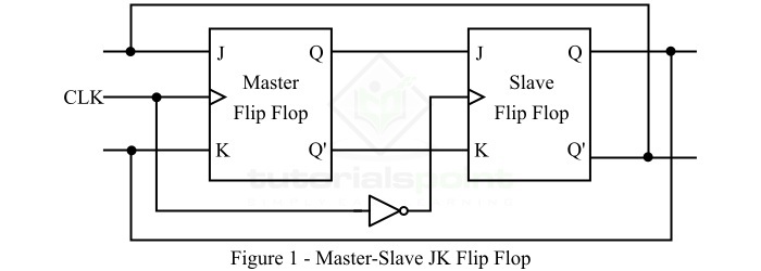
In this combination of two JK flip flop, one acts as a master flip flop and the other acts as a slave flip flop. In this master-slave flip flop, the outputs of the master JK flip flop are connected to the inputs of the slave JK flip flop. The outputs of the slave flip flop are fed back to the inputs of the master JK flip flop.
In the master-slave JK flip flop, a NOT gate (Inverter) is also used which is connected to clock signal in a manner that the inverted clock signal is applied to the slave flip flop.
Therefore, when clock signal to master flip flop is 0, then for slave flip flop the clock signal is 1, and if the clock signal to master flip flop is 1, then for the slave flip flop it 0.
Operation of Master-Slave JK Flip Flop
When the clock pulse goes to high, the slave flip flop becomes inactive and the inputs J and K can control the state of the system.
When the clock pulse goes back to low, the information is transferred from master flip flop to the slave flip flop, and the final output of the system is obtained.
From the circuit, it is clear that the master flip flop is positive level triggered and the slave flip flop is negative level triggered. Consequently, the master flip flop responds before the slave flip flop. Now, let us discuss the operation of the master-slave JK flip flop for different combinations of inputs J and K.
- When J = 0 and K = 0, both JK flip flops remains inactive and hence the output Q remains unchanged. This is called Hold State of the master-slave JK flip flop.
- When J = 0 and K = 1, the output Q' of the master flip flop is high and goes to the input K of the slave flip flop. The clock signal forces the slave flip flop to reset. Therefore, the slave flip flop has the same output has the master flip flop, i.e., high Q' and low Q. This is called reset state of the master-slave JK flip flop.
- When J = 1 and K = 0, the output Q of the master flip flop is high and goes to the input J of the slave flip flop, the negative transition of the clock signal sets the slave flip flop. Hence, this is called the set state of the master-slave JK flip flop.
- When J = 1 and K = 1, for this input combination, the master flip flop toggles on the positive transition of the clock pulse and the slave flip flop toggles on the negative transition of the clock pulse. Hence, the problem of the race around condition of the JK flip flop is solved.
Truth Table of Master-Slave JK Flip Flop
The following is the truth table of the master-slave JK flip flop
| Inputs | Output | Comment | |
|---|---|---|---|
| J | K | Qn+1 | |
| 0 | 0 | Qn | No Change |
| 0 | 1 | 0 | Reset |
| 1 | 0 | 1 | Set |
| 1 | 1 | Qn' | Toggle |
This is all about the master-slave JK flip-flop and its operation.