- Digital Electronics - Home
- Digital Electronics Basics
- Types of Digital Systems
- Types of Signals
- Logic Levels And Pulse Waveforms
- Digital System Components
- Digital Logic Operations
- Digital Systems Advantages
- Number Systems
- Number Systems
- Binary Numbers Representation
- Binary Arithmetic
- Signed Binary Arithmetic
- Octal Arithmetic
- Hexadecimal Arithmetic
- Complement Arithmetic
- Base Conversions
- Base Conversions
- Binary to Decimal Conversion
- Decimal to Binary Conversion
- Binary to Octal Conversion
- Octal to Binary Conversion
- Octal to Decimal Conversion
- Decimal to Octal Conversion
- Hexadecimal to Binary Conversion
- Binary to Hexadecimal Conversion
- Hexadecimal to Decimal Conversion
- Decimal to Hexadecimal Conversion
- Octal to Hexadecimal Conversion
- Hexadecimal to Octal Conversion
- Binary Codes
- Binary Codes
- 8421 BCD Code
- Excess-3 Code
- Gray Code
- ASCII Codes
- EBCDIC Code
- Code Conversion
- Error Detection & Correction Codes
- Logic Gates
- Logic Gates
- AND Gate
- OR Gate
- NOT Gate
- Universal Gates
- XOR Gate
- XNOR Gate
- CMOS Logic Gate
- OR Gate Using Diode Resistor Logic
- AND Gate vs OR Gate
- Two Level Logic Realization
- Threshold Logic
- Boolean Algebra
- Boolean Algebra
- Laws of Boolean Algebra
- Boolean Functions
- DeMorgan's Theorem
- SOP and POS Form
- POS to Standard POS Form
- Minimization Techniques
- K-Map Minimization
- Three Variable K-Map
- Four Variable K-Map
- Five Variable K-Map
- Six Variable K-Map
- Don't Care Condition
- Quine-McCluskey Method
- Min Terms and Max Terms
- Canonical and Standard Form
- Max Term Representation
- Simplification using Boolean Algebra
- Combinational Logic Circuits
- Digital Combinational Circuits
- Digital Arithmetic Circuits
- Multiplexers
- Multiplexer Design Procedure
- Mux Universal Gate
- 2-Variable Function Using 4:1 Mux
- 3-Variable Function Using 8:1 Mux
- Demultiplexers
- Mux vs Demux
- Parity Bit Generator and Checker
- Comparators
- Encoders
- Keyboard Encoders
- Priority Encoders
- Decoders
- Arithmetic Logic Unit
- 7-Segment LED Display
- Code Converters
- Code Converters
- Binary to Decimal Converter
- Decimal to BCD Converter
- BCD to Decimal Converter
- Binary to Gray Code Converter
- Gray Code to Binary Converter
- BCD to Excess-3 Converter
- Excess-3 to BCD Converter
- Adders
- Half Adders
- Full Adders
- Serial Adders
- Parallel Adders
- Full Adder using Half Adder
- Half Adder vs Full Adder
- Full Adder with NAND Gates
- Half Adder with NAND Gates
- Binary Adder-Subtractor
- Subtractors
- Half Subtractors
- Full Subtractors
- Parallel Subtractors
- Full Subtractor using 2 Half Subtractors
- Half Subtractor using NAND Gates
- Sequential Logic Circuits
- Digital Sequential Circuits
- Clock Signal and Triggering
- Latches
- Shift Registers
- Shift Register Applications
- Binary Registers
- Bidirectional Shift Register
- Counters
- Binary Counters
- Non-binary Counter
- Design of Synchronous Counter
- Synchronous vs Asynchronous Counter
- Finite State Machines
- Algorithmic State Machines
- Flip Flops
- Flip-Flops
- Conversion of Flip-Flops
- D Flip-Flops
- JK Flip-Flops
- T Flip-Flops
- SR Flip-Flops
- Clocked SR Flip-Flop
- Unclocked SR Flip-Flop
- Clocked JK Flip-Flop
- JK to T Flip-Flop
- SR to JK Flip-Flop
- Triggering Methods:Flip-Flop
- Edge-Triggered Flip-Flop
- Master-Slave JK Flip-Flop
- Race-around Condition
- A/D and D/A Converters
- Analog-to-Digital Converter
- Digital-to-Analog Converter
- DAC and ADC ICs
- Realization of Logic Gates
- NOT Gate from NAND Gate
- OR Gate from NAND Gate
- AND Gate from NAND Gate
- NOR Gate from NAND Gate
- XOR Gate from NAND Gate
- XNOR Gate from NAND Gate
- NOT Gate from NOR Gate
- OR Gate from NOR Gate
- AND Gate from NOR Gate
- NAND Gate from NOR Gate
- XOR Gate from NOR Gate
- XNOR Gate from NOR Gate
- NAND/NOR Gate using CMOS
- Full Subtractor using NAND Gate
- AND Gate Using 2:1 MUX
- OR Gate Using 2:1 MUX
- NOT Gate Using 2:1 MUX
- Memory Devices
- Memory Devices
- RAM and ROM
- Cache Memory Design
- Programmable Logic Devices
- Programmable Logic Devices
- Programmable Logic Array
- Programmable Array Logic
- Field Programmable Gate Arrays
- Digital Electronics Families
- Digital Electronics Families
- CPU Architecture
- CPU Architecture
Multiplexer Universal Logic Gate
Read this chapter to learn how you can use a multiplexer to realize universal logic gates. Let us start with a brief introduction to multiplexers and universal logic gates.
What is a Multiplexer?
A Multiplexer or MUX or Data Selector is a combinational logic circuit which accepts several data inputs and allows only one of them at a time to pass through the output channel. The block diagram of a multiplexer is shown in Figure-1.
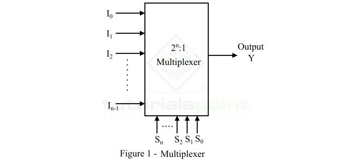
A multiplexer consists 2n data input lines, n select lines, and only one output line. The logic level applied to the select lines determine which input will pass to the output channel.
Depending on the number of data input lines, multiplexers can be of several types such as 2:1 MUX, 4:1 MUX, 8:1 MUX, etc. In digital electronics, multiplexers are used in several application like realization of Boolean functions and different types of logic gates.
What is a Universal Gate?
A Universal Logic Gate is a type of logic gate (a digital device used to perform a logical operation) which can be used to implement any kind of logic function or other basic logic gates such as OR, AND, NOT, etc.
In digital electronics, we have two universal logic gates namely, NAND Gate and NOR Gate.
NAND Gate
The NAND Gate is a type of universal logic gate. The NAND gate is basically a combination of two basic logic gates namely AND gate and NOT gate, i.e.,
NAND Logic = AND Logic + NOT Logic
The NAND gate is the logic gate whose output is LOW when all its inputs are high, and its output is HIGH, when any of its inputs is LOW. Therefore, the operation of the NAND gate is opposite that of the AND gate. The logic symbol of a two input NAND gate is shown in Figure-2.

For the NAND gate, if A and B are the input variables and Y is the output variable, then its output equation is given by,
$$\mathrm{Y \: = \: \overline{A \: \cdot \: B} \: = \: \left ( A \: \cdot \: B \right )'}$$
It is read as "Y is equal to A.B whole bar".
The operation of the NAND gate for different possible combinations of inputs can be analyzed with the help its truth table which is given below −
| Inputs | Output | |
|---|---|---|
| A | B | Y = (A.B)' |
| 0 | 0 | 1 |
| 0 | 1 | 1 |
| 1 | 0 | 1 |
| 1 | 1 | 0 |
NOR Gate
The NOR Gate is another type of universal logic gate. Here, NOR means NOT + OR. That means, the OR output is NOTed or inverted. Thus, the NOR gate is a combination of OR gate and a NOT gate, i.e.,
NOR Gate = OR Gate + NOT Gate
The NOR gate is a logic gate whose output is HIGH, only when all its inputs are LOW, and it gives an output LOW, even if any of its inputs becomes HIGH. The logic symbol of a two input NOR gate is shown in Figure-3.

For a NOR gate, if A and B are the input variables and Y is the output variable, then the output equation of the NOR gate is given by,
$$\mathrm{Y \: = \: \overline{A \: + \: B} \: = \: \left ( A \: + \: B \right )'}$$
It is read as "Y is equal to A plus B whole bar".
We can analyze the operation of the NOR gate for different possible combinations of inputs by its truth table which is given below −
| Inputs | Output | |
|---|---|---|
| A | B | Y = (A+B)' |
| 0 | 0 | 1 |
| 0 | 1 | 0 |
| 1 | 0 | 0 |
| 1 | 1 | 0 |
Now, after getting a brief description about multiplexer, NAND gate and NOR gate. We can discuss the implementation of these universal logic gates using multiplexer.
NAND Gate using Multiplexer
The implementation of a two input NAND gate using multiplexer is shown in Figure-4.
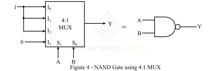
Since a two input NAND gate can have total four (22 = 4) possible combinations of input variables. Hence, to realize a two input NAND gate, we require a 4:1 MUX.
According the truth table of two input NAND gate, the output Y = 1 for first three combinations, i.e. 00, 01, 10. Thus, the input lines I0, I1, and I2 of the multiplexer are connected to logic 1. The output of the NAND gate Y = 0 for combination 11, thus, the input line I3 of MUX is connected to logic 0.
In this way, we can realize the NAND gate using a multiplexer. Now, let us discuss the implementation of NOR gate using multiplexer.
NOR Gate using Multiplexer
The implementation of a two input NOR gate using a multiplexer is shown in Figure-5.
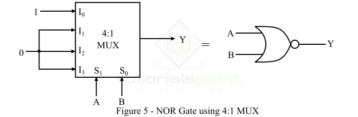
Since a two input NOR gate can have total four (22 = 4) possible combinations of input variables. Hence, to realize a two input NOR gate, we require a 4:1 MUX.
The input variables A and B of the NOR gate are used as the select lines of the multiplexer. Where, A and B are applied to S1 and S0 respectively.
As per the truth table of the two input NOR gate, the output Y = 1 for only first combination of input variables, i.e. 00. Hence, we apply logic 1 only to the data input line I0 of the multiplexer. The output of the NOR gate Y = 0 for all other combinations, i.e. 01, 10, and 11, therefore, the input lines I1, I2, and I3 of the MUX are connected to logic 0. This way, a NOR gate can be realized using a multiplexer.
Solving Problems
Try to solve the following tutorial problems to excel in the concept of using a multiplexer to realize universal logic gates.
Q. 1 − Implement a three input NAND gate using an 8:1 MUX.
Q. 2 − Implement a three variable NOR gate by using an 8:1 MUX.