- Digital Electronics - Home
- Digital Electronics Basics
- Types of Digital Systems
- Types of Signals
- Logic Levels And Pulse Waveforms
- Digital System Components
- Digital Logic Operations
- Digital Systems Advantages
- Number Systems
- Number Systems
- Binary Numbers Representation
- Binary Arithmetic
- Signed Binary Arithmetic
- Octal Arithmetic
- Hexadecimal Arithmetic
- Complement Arithmetic
- Base Conversions
- Base Conversions
- Binary to Decimal Conversion
- Decimal to Binary Conversion
- Binary to Octal Conversion
- Octal to Binary Conversion
- Octal to Decimal Conversion
- Decimal to Octal Conversion
- Hexadecimal to Binary Conversion
- Binary to Hexadecimal Conversion
- Hexadecimal to Decimal Conversion
- Decimal to Hexadecimal Conversion
- Octal to Hexadecimal Conversion
- Hexadecimal to Octal Conversion
- Binary Codes
- Binary Codes
- 8421 BCD Code
- Excess-3 Code
- Gray Code
- ASCII Codes
- EBCDIC Code
- Code Conversion
- Error Detection & Correction Codes
- Logic Gates
- Logic Gates
- AND Gate
- OR Gate
- NOT Gate
- Universal Gates
- XOR Gate
- XNOR Gate
- CMOS Logic Gate
- OR Gate Using Diode Resistor Logic
- AND Gate vs OR Gate
- Two Level Logic Realization
- Threshold Logic
- Boolean Algebra
- Boolean Algebra
- Laws of Boolean Algebra
- Boolean Functions
- DeMorgan's Theorem
- SOP and POS Form
- POS to Standard POS Form
- Minimization Techniques
- K-Map Minimization
- Three Variable K-Map
- Four Variable K-Map
- Five Variable K-Map
- Six Variable K-Map
- Don't Care Condition
- Quine-McCluskey Method
- Min Terms and Max Terms
- Canonical and Standard Form
- Max Term Representation
- Simplification using Boolean Algebra
- Combinational Logic Circuits
- Digital Combinational Circuits
- Digital Arithmetic Circuits
- Multiplexers
- Multiplexer Design Procedure
- Mux Universal Gate
- 2-Variable Function Using 4:1 Mux
- 3-Variable Function Using 8:1 Mux
- Demultiplexers
- Mux vs Demux
- Parity Bit Generator and Checker
- Comparators
- Encoders
- Keyboard Encoders
- Priority Encoders
- Decoders
- Arithmetic Logic Unit
- 7-Segment LED Display
- Code Converters
- Code Converters
- Binary to Decimal Converter
- Decimal to BCD Converter
- BCD to Decimal Converter
- Binary to Gray Code Converter
- Gray Code to Binary Converter
- BCD to Excess-3 Converter
- Excess-3 to BCD Converter
- Adders
- Half Adders
- Full Adders
- Serial Adders
- Parallel Adders
- Full Adder using Half Adder
- Half Adder vs Full Adder
- Full Adder with NAND Gates
- Half Adder with NAND Gates
- Binary Adder-Subtractor
- Subtractors
- Half Subtractors
- Full Subtractors
- Parallel Subtractors
- Full Subtractor using 2 Half Subtractors
- Half Subtractor using NAND Gates
- Sequential Logic Circuits
- Digital Sequential Circuits
- Clock Signal and Triggering
- Latches
- Shift Registers
- Shift Register Applications
- Binary Registers
- Bidirectional Shift Register
- Counters
- Binary Counters
- Non-binary Counter
- Design of Synchronous Counter
- Synchronous vs Asynchronous Counter
- Finite State Machines
- Algorithmic State Machines
- Flip Flops
- Flip-Flops
- Conversion of Flip-Flops
- D Flip-Flops
- JK Flip-Flops
- T Flip-Flops
- SR Flip-Flops
- Clocked SR Flip-Flop
- Unclocked SR Flip-Flop
- Clocked JK Flip-Flop
- JK to T Flip-Flop
- SR to JK Flip-Flop
- Triggering Methods:Flip-Flop
- Edge-Triggered Flip-Flop
- Master-Slave JK Flip-Flop
- Race-around Condition
- A/D and D/A Converters
- Analog-to-Digital Converter
- Digital-to-Analog Converter
- DAC and ADC ICs
- Realization of Logic Gates
- NOT Gate from NAND Gate
- OR Gate from NAND Gate
- AND Gate from NAND Gate
- NOR Gate from NAND Gate
- XOR Gate from NAND Gate
- XNOR Gate from NAND Gate
- NOT Gate from NOR Gate
- OR Gate from NOR Gate
- AND Gate from NOR Gate
- NAND Gate from NOR Gate
- XOR Gate from NOR Gate
- XNOR Gate from NOR Gate
- NAND/NOR Gate using CMOS
- Full Subtractor using NAND Gate
- AND Gate Using 2:1 MUX
- OR Gate Using 2:1 MUX
- NOT Gate Using 2:1 MUX
- Memory Devices
- Memory Devices
- RAM and ROM
- Cache Memory Design
- Programmable Logic Devices
- Programmable Logic Devices
- Programmable Logic Array
- Programmable Array Logic
- Field Programmable Gate Arrays
- Digital Electronics Families
- Digital Electronics Families
- CPU Architecture
- CPU Architecture
Race-around Condition in JK Flip-flop
Let's start this chapter with a brief introduction of JK flip-flop and its block diagram and truth table, before moving on to discuss the race-around condition.
JK Flip-Flop
JK flip-flops is a one-bit storage device which has two stable states. The block diagram representation of a JK flip-flops is shown in Figure-1.

It has two inputs specified by "J" and "K", one clock input for synchronization of the circuit, and two outputs represented by Q and Q'.
When clock signal is absent, the output of the JK flip-flop is independent of the inputs J and K. When the clock signal is present, the output of the JK flip-flops changes according to the inputs J and K.
Truth Table of JK Flip-Flop
The operation of the JK flip-flops can be studied from its truth table which is given as follows −
| Inputs | Previous State | Output (Next State) | Comment | |
|---|---|---|---|---|
| J | K | Qn | Qn+1 | |
| 0 | 0 | 0 | 0 | No Change |
| 0 | 0 | 1 | 1 | No Change |
| 0 | 1 | 0 | 0 | Reset |
| 0 | 1 | 1 | 0 | Reset |
| 1 | 0 | 0 | 1 | Set |
| 1 | 0 | 1 | 1 | Set |
| 1 | 1 | 0 | 1 | Toggle |
| 1 | 1 | 1 | 0 | Toggle |
Now, let us discuss the race-around condition in the JK flip-flops.
Race-around Condition in JK Flip-flops
From the above truth table of the JK flip-flops, it can be observed that when J = 1 and K =1, then output Qn+1 = Qn', which means for inputs J = 1 and K = 1, the JK flip-flops acts as a toggle switch.
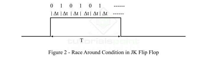
Let us consider the inputs J = 1 and K = 1, and the output Q = 0. After the propagation delay (let t) of the flip-flops, the output of the JK flip-flops changes from 0 to 1. As we know, the output of the JK flip-flops is connected to its inputs. Hence, the output also acts as input, and thus after the next delay (t), the output will change from 1 to 0. This process will continue till the end of the applied clock signal. Thus, the output of the JK flip-flops is uncertain. This condition of JK flip-flops is called the race-around condition.
Race-around condition in JK flip-flops is shown in Figure-2, where T is the total duration of clock pulse.
How the Race-around Condition Can be Avoided?
The problem of the race-around condition does not exist in the flip-flops where the inputs do not change during the presence of clock pulse. But, in the case of JK flip-flops, the inputs change during the clock pulse due to the feedback path present between inputs and outputs. Hence, in JK flip-flops, the race around condition is a major problem.
The problem of race-around condition and the uncertainty of output can be avoided by increasing the delay of the flip-flops. For that, the delay of the flip-flops must be greater than the duration of the clock signal, i.e. t > T. In another way, the duration of the applied clock signal (T) must be reduced to make it less than the delay of the flip-flops (t).
However, the increase in the delay of the flip-flops is not a good practice because it decreases the speed of the system. On the other hand, it is also quite difficult to decrease the duration of the clock pulse (T) beyond the delay of the flip-flops (t). This is because, the delay of the JK flip-flops (t) is of the order of nanoseconds.
Hence, the most practical way to solve the problem of race-around condition in JK flip-flops is to use the JK flip-flops in the Master and Slave Mode. In the master-slave mode of JK flip-flops, two JK flip-flops are cascaded.
This is all about the race-around condition and its remedies in JK flip-flops.