- Digital Electronics - Home
- Digital Electronics Basics
- Types of Digital Systems
- Types of Signals
- Logic Levels And Pulse Waveforms
- Digital System Components
- Digital Logic Operations
- Digital Systems Advantages
- Number Systems
- Number Systems
- Binary Numbers Representation
- Binary Arithmetic
- Signed Binary Arithmetic
- Octal Arithmetic
- Hexadecimal Arithmetic
- Complement Arithmetic
- Base Conversions
- Base Conversions
- Binary to Decimal Conversion
- Decimal to Binary Conversion
- Binary to Octal Conversion
- Octal to Binary Conversion
- Octal to Decimal Conversion
- Decimal to Octal Conversion
- Hexadecimal to Binary Conversion
- Binary to Hexadecimal Conversion
- Hexadecimal to Decimal Conversion
- Decimal to Hexadecimal Conversion
- Octal to Hexadecimal Conversion
- Hexadecimal to Octal Conversion
- Binary Codes
- Binary Codes
- 8421 BCD Code
- Excess-3 Code
- Gray Code
- ASCII Codes
- EBCDIC Code
- Code Conversion
- Error Detection & Correction Codes
- Logic Gates
- Logic Gates
- AND Gate
- OR Gate
- NOT Gate
- Universal Gates
- XOR Gate
- XNOR Gate
- CMOS Logic Gate
- OR Gate Using Diode Resistor Logic
- AND Gate vs OR Gate
- Two Level Logic Realization
- Threshold Logic
- Boolean Algebra
- Boolean Algebra
- Laws of Boolean Algebra
- Boolean Functions
- DeMorgan's Theorem
- SOP and POS Form
- POS to Standard POS Form
- Minimization Techniques
- K-Map Minimization
- Three Variable K-Map
- Four Variable K-Map
- Five Variable K-Map
- Six Variable K-Map
- Don't Care Condition
- Quine-McCluskey Method
- Min Terms and Max Terms
- Canonical and Standard Form
- Max Term Representation
- Simplification using Boolean Algebra
- Combinational Logic Circuits
- Digital Combinational Circuits
- Digital Arithmetic Circuits
- Multiplexers
- Multiplexer Design Procedure
- Mux Universal Gate
- 2-Variable Function Using 4:1 Mux
- 3-Variable Function Using 8:1 Mux
- Demultiplexers
- Mux vs Demux
- Parity Bit Generator and Checker
- Comparators
- Encoders
- Keyboard Encoders
- Priority Encoders
- Decoders
- Arithmetic Logic Unit
- 7-Segment LED Display
- Code Converters
- Code Converters
- Binary to Decimal Converter
- Decimal to BCD Converter
- BCD to Decimal Converter
- Binary to Gray Code Converter
- Gray Code to Binary Converter
- BCD to Excess-3 Converter
- Excess-3 to BCD Converter
- Adders
- Half Adders
- Full Adders
- Serial Adders
- Parallel Adders
- Full Adder using Half Adder
- Half Adder vs Full Adder
- Full Adder with NAND Gates
- Half Adder with NAND Gates
- Binary Adder-Subtractor
- Subtractors
- Half Subtractors
- Full Subtractors
- Parallel Subtractors
- Full Subtractor using 2 Half Subtractors
- Half Subtractor using NAND Gates
- Sequential Logic Circuits
- Digital Sequential Circuits
- Clock Signal and Triggering
- Latches
- Shift Registers
- Shift Register Applications
- Binary Registers
- Bidirectional Shift Register
- Counters
- Binary Counters
- Non-binary Counter
- Design of Synchronous Counter
- Synchronous vs Asynchronous Counter
- Finite State Machines
- Algorithmic State Machines
- Flip Flops
- Flip-Flops
- Conversion of Flip-Flops
- D Flip-Flops
- JK Flip-Flops
- T Flip-Flops
- SR Flip-Flops
- Clocked SR Flip-Flop
- Unclocked SR Flip-Flop
- Clocked JK Flip-Flop
- JK to T Flip-Flop
- SR to JK Flip-Flop
- Triggering Methods:Flip-Flop
- Edge-Triggered Flip-Flop
- Master-Slave JK Flip-Flop
- Race-around Condition
- A/D and D/A Converters
- Analog-to-Digital Converter
- Digital-to-Analog Converter
- DAC and ADC ICs
- Realization of Logic Gates
- NOT Gate from NAND Gate
- OR Gate from NAND Gate
- AND Gate from NAND Gate
- NOR Gate from NAND Gate
- XOR Gate from NAND Gate
- XNOR Gate from NAND Gate
- NOT Gate from NOR Gate
- OR Gate from NOR Gate
- AND Gate from NOR Gate
- NAND Gate from NOR Gate
- XOR Gate from NOR Gate
- XNOR Gate from NOR Gate
- NAND/NOR Gate using CMOS
- Full Subtractor using NAND Gate
- AND Gate Using 2:1 MUX
- OR Gate Using 2:1 MUX
- NOT Gate Using 2:1 MUX
- Memory Devices
- Memory Devices
- RAM and ROM
- Cache Memory Design
- Programmable Logic Devices
- Programmable Logic Devices
- Programmable Logic Array
- Programmable Array Logic
- Field Programmable Gate Arrays
- Digital Electronics Families
- Digital Electronics Families
- CPU Architecture
- CPU Architecture
Digital Electronics - Conversion of Flip-Flops
In previous chapter, we discussed the four flip-flops, namely SR flip-flop, D flip-flop, JK flip-flop & T flip-flop. We can convert one flip-flop into the remaining three flip-flops by including some additional logic. So, there will be total of twelve flip-flop conversions.
Follow these steps for converting one flip-flop to the other.
- Consider the characteristic table of desired flip-flop.
- Fill the excitation values (inputs) of given flip-flop for each combination of present state and next state. The excitation table for all flip-flops is shown below.
| Present State | Next State | SR Flip-Flop Inputs | D flip-flop input | JK Flip-Flop Inputs | T Flip-Flop Input | ||
|---|---|---|---|---|---|---|---|
| Q(t) | Q(t+1) | S | R | D | J | K | T |
| 0 | 0 | 0 | x | 0 | 0 | x | 0 |
| 0 | 1 | 1 | 0 | 1 | 1 | x | 1 |
| 1 | 0 | 0 | 1 | 0 | x | 1 | 1 |
| 1 | 1 | x | 0 | 1 | x | 0 | 0 |
Get the simplified expressions for each excitation input. If necessary, use Kmaps for simplifying.
Draw the circuit diagram of desired flip-flop according to the simplified expressions using given flip-flop and necessary logic gates.
Now, let us convert few flip-flops into other. Follow the same process for remaining flipflop conversions.
SR Flip-Flop to other Flip-Flop Conversions
Following are the three possible conversions of SR flip-flop to other flip-flops.
- SR Flip-Flop to D Flip-Flop
- SR Flip-Flop to JK Flip-Flop
- SR Flip-Flop to T Flip-Flop
SR Flip-Flop to D Flip-Flop Conversion
Here, the given flip-flop is SR flip-flop and the desired flip-flop is D flip-flop. Therefore, consider the following characteristic table of D flip-flop.
| D Flip-Flop Input | Present State | Next State |
|---|---|---|
| D | Q(t) | Q(t + 1) |
| 0 | 0 | 0 |
| 0 | 1 | 0 |
| 1 | 0 | 1 |
| 1 | 1 | 1 |
We know that SR flip-flop has two inputs S & R. So, write down the excitation values of SR flip-flop for each combination of present state and next state values. The following table shows the characteristic table of D flip-flop along with the excitation inputs of SR flip-flop.
| D Flip-Flop Input | Present State | Next State | SR Flip-Flop Inputs | |
|---|---|---|---|---|
| D | Q(t) | Q(t + 1) | S | R |
| 0 | 0 | 0 | 0 | x |
| 0 | 1 | 0 | 0 | 1 |
| 1 | 0 | 1 | 1 | 0 |
| 1 | 1 | 1 | x | 0 |
From the above table, we can write the Boolean functions for each input as below.
$$\mathrm{S \: = \: m_{2} \: + \: d_{3}}$$
$$\mathrm{R \: = \: m_{1} \: + \: d_{0}}$$
We can use 2 variable K-Maps for getting simplified expressions for these inputs. The k-Maps for S & R are shown below.
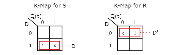
So, we got S = D & R = D' after simplifying. The circuit diagram of D flip-flop is shown in the following figure.
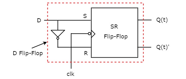
This circuit consists of SR flip-flop and an inverter. This inverter produces an output, which is complement of input, D. So, the overall circuit has single input, D and two outputs Q(t) & Q(t)'. Hence, it is a D flip-flop. Similarly, you can do other two conversions.
D Flip-Flop to other Flip-Flop Conversions
Following are the three possible conversions of D flip-flop to other flip-flops.
- D Flip-Flop to T Flip-Flop
- D Flip-Flop to SR Flip-Flop
- D Flip-Flop to JK Flip-Flop
D Flip-Flop to T Flip-Flop conversion
Here, the given flip-flop is D flip-flop and the desired flip-flop is T flip-flop. Therefore, consider the following characteristic table of T flip-flop.
| T Flip-Flop Input | Present State | Next State |
|---|---|---|
| T | Q(t) | Q(t + 1) |
| 0 | 0 | 0 |
| 0 | 1 | 1 |
| 1 | 0 | 1 |
| 1 | 1 | 0 |
We know that D flip-flop has single input D. So, write down the excitation values of D flip-flop for each combination of present state and next state values. The following table shows the characteristic table of T flip-flop along with the excitation input of D flip-flop.
| T Flip-Flop Input | Present State | Next State | D Flip-Flop Input |
|---|---|---|---|
| T | Q(t) | Q(t + 1) | D |
| 0 | 0 | 0 | 0 |
| 0 | 1 | 1 | 1 |
| 1 | 0 | 1 | 1 |
| 1 | 1 | 0 | 0 |
From the above table, we can directly write the Boolean function of D as below.
$$\mathrm{D \: = \: T \: \oplus \: Q \: \left ( t \: \right )}$$
So, we require a two input Exclusive-OR gate along with D flip-flop. The circuit diagram of T flip-flop is shown in the following figure.

This circuit consists of D flip-flop and an Exclusive-OR gate. This Exclusive-OR gate produces an output, which is Ex-OR of T and Q(t). So, the overall circuit has single input, T and two outputs Q(t) & Q(t). Hence, it is a T flip-flop. Similarly, you can do other two conversions.
JK Flip-Flop to other Flip-Flop Conversions
Following are the three possible conversions of JK flip-flop to other flip-flops.
- JK Flip-Flop to T Flip-Flop
- JK Flip-Flop to D Flip-Flop
- JK Flip-Flop to SR Flip-Flop
JK Flip-Flop to T Flip-Flop conversion
Here, the given flip-flop is JK flip-flop and the desired flip-flop is T flip-flop. Therefore, consider the following characteristic table of T flip-flop.
| T Flip-Flop Input | Present State | Next State |
|---|---|---|
| T | Q(t) | Q(t + 1) |
| 0 | 0 | 0 |
| 0 | 1 | 1 |
| 1 | 0 | 1 |
| 1 | 1 | 0 |
We know that JK flip-flop has two inputs J & K. So, write down the excitation values of JK flip-flop for each combination of present state and next state values. The following table shows the characteristic table of T flip-flop along with the excitation inputs of JK flipflop.
| T Flip-Flop Input | Present State | Next State | JK Flip-Flop Inputs | |
|---|---|---|---|---|
| T | Q(t) | Q(t + 1) | J | K |
| 0 | 0 | 0 | 0 | x |
| 0 | 1 | 1 | x | 0 |
| 1 | 0 | 1 | 1 | x |
| 1 | 1 | 0 | x | 1 |
From the above table, we can write the Boolean functions for each input as below.
$$\mathrm{J \: = \: m_{2} \: + \: d_{1} \: + \: d_{3}}$$
$$\mathrm{K \: = \: m_{3} \: + \: d_{0} \: + \: d_{2}}$$
We can use 2 variable K-Maps for getting simplified expressions for these two inputs. The k-Maps for J & K are shown below.
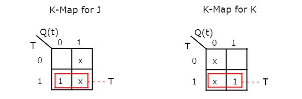
So, we got, J = T & K = T after simplifying. The circuit diagram of T flip-flop is shown in the following figure.
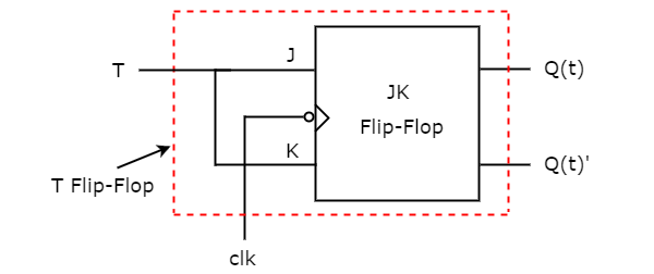
This circuit consists of JK flip-flop only. It doesnt require any other gates. Just connect the same input T to both J & K. So, the overall circuit has single input, T and two outputs Q(t) & Q(t). Hence, it is a T flip-flop. Similarly, you can do other two conversions.
T Flip-Flop to other Flip-Flop Conversions
Following are the three possible conversions of T flip-flop to other flip-flops.
- T Flip-Flop to D Flip-Flop
- T Flip-Flop to SR Flip-Flop
- T Flip-Flop to JK Flip-Flop
T Flip-Flop to D Flip-Flop conversion
Here, the given flip-flop is T flip-flop and the desired flip-flop is D flip-flop. Therefore, consider the characteristic table of D flip-flop and write down the excitation values of T flip-flop for each combination of present state and next state values. The following table shows the characteristic table of D flip-flop along with the excitation input of T flip-flop.
| D Flip-Flop Input | Present State | Next State | T Flip-Flop Input | |
|---|---|---|---|---|
| D | Q(t) | Q(t + 1) | T | |
| 0 | 0 | 0 | 0 | |
| 0 | 1 | 0 | 1 | |
| 1 | 0 | 1 | 1 | |
| 1 | 1 | 1 | 0 | |
From the above table, we can directly write the Boolean function of T as below.
$$\mathrm{T \: = \: D \: \oplus \: Q \left ( t \right )}$$
So, we require a two input Exclusive-OR gate along with T flip-flop. The circuit diagram of D flip-flop is shown in the following figure.
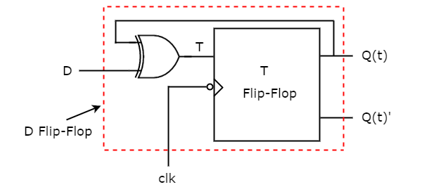
This circuit consists of T flip-flop and an Exclusive-OR gate. This Exclusive-OR gate produces an output, which is Ex-OR of D and Q(t). So, the overall circuit has single input, D and two outputs Q(t) & Q(t). Hence, it is a D flip-flop. Similarly, you can do other two conversions.