- Digital Electronics - Home
- Digital Electronics Basics
- Types of Digital Systems
- Types of Signals
- Logic Levels And Pulse Waveforms
- Digital System Components
- Digital Logic Operations
- Digital Systems Advantages
- Number Systems
- Number Systems
- Binary Numbers Representation
- Binary Arithmetic
- Signed Binary Arithmetic
- Octal Arithmetic
- Hexadecimal Arithmetic
- Complement Arithmetic
- Base Conversions
- Base Conversions
- Binary to Decimal Conversion
- Decimal to Binary Conversion
- Binary to Octal Conversion
- Octal to Binary Conversion
- Octal to Decimal Conversion
- Decimal to Octal Conversion
- Hexadecimal to Binary Conversion
- Binary to Hexadecimal Conversion
- Hexadecimal to Decimal Conversion
- Decimal to Hexadecimal Conversion
- Octal to Hexadecimal Conversion
- Hexadecimal to Octal Conversion
- Binary Codes
- Binary Codes
- 8421 BCD Code
- Excess-3 Code
- Gray Code
- ASCII Codes
- EBCDIC Code
- Code Conversion
- Error Detection & Correction Codes
- Logic Gates
- Logic Gates
- AND Gate
- OR Gate
- NOT Gate
- Universal Gates
- XOR Gate
- XNOR Gate
- CMOS Logic Gate
- OR Gate Using Diode Resistor Logic
- AND Gate vs OR Gate
- Two Level Logic Realization
- Threshold Logic
- Boolean Algebra
- Boolean Algebra
- Laws of Boolean Algebra
- Boolean Functions
- DeMorgan's Theorem
- SOP and POS Form
- POS to Standard POS Form
- Minimization Techniques
- K-Map Minimization
- Three Variable K-Map
- Four Variable K-Map
- Five Variable K-Map
- Six Variable K-Map
- Don't Care Condition
- Quine-McCluskey Method
- Min Terms and Max Terms
- Canonical and Standard Form
- Max Term Representation
- Simplification using Boolean Algebra
- Combinational Logic Circuits
- Digital Combinational Circuits
- Digital Arithmetic Circuits
- Multiplexers
- Multiplexer Design Procedure
- Mux Universal Gate
- 2-Variable Function Using 4:1 Mux
- 3-Variable Function Using 8:1 Mux
- Demultiplexers
- Mux vs Demux
- Parity Bit Generator and Checker
- Comparators
- Encoders
- Keyboard Encoders
- Priority Encoders
- Decoders
- Arithmetic Logic Unit
- 7-Segment LED Display
- Code Converters
- Code Converters
- Binary to Decimal Converter
- Decimal to BCD Converter
- BCD to Decimal Converter
- Binary to Gray Code Converter
- Gray Code to Binary Converter
- BCD to Excess-3 Converter
- Excess-3 to BCD Converter
- Adders
- Half Adders
- Full Adders
- Serial Adders
- Parallel Adders
- Full Adder using Half Adder
- Half Adder vs Full Adder
- Full Adder with NAND Gates
- Half Adder with NAND Gates
- Binary Adder-Subtractor
- Subtractors
- Half Subtractors
- Full Subtractors
- Parallel Subtractors
- Full Subtractor using 2 Half Subtractors
- Half Subtractor using NAND Gates
- Sequential Logic Circuits
- Digital Sequential Circuits
- Clock Signal and Triggering
- Latches
- Shift Registers
- Shift Register Applications
- Binary Registers
- Bidirectional Shift Register
- Counters
- Binary Counters
- Non-binary Counter
- Design of Synchronous Counter
- Synchronous vs Asynchronous Counter
- Finite State Machines
- Algorithmic State Machines
- Flip Flops
- Flip-Flops
- Conversion of Flip-Flops
- D Flip-Flops
- JK Flip-Flops
- T Flip-Flops
- SR Flip-Flops
- Clocked SR Flip-Flop
- Unclocked SR Flip-Flop
- Clocked JK Flip-Flop
- JK to T Flip-Flop
- SR to JK Flip-Flop
- Triggering Methods:Flip-Flop
- Edge-Triggered Flip-Flop
- Master-Slave JK Flip-Flop
- Race-around Condition
- A/D and D/A Converters
- Analog-to-Digital Converter
- Digital-to-Analog Converter
- DAC and ADC ICs
- Realization of Logic Gates
- NOT Gate from NAND Gate
- OR Gate from NAND Gate
- AND Gate from NAND Gate
- NOR Gate from NAND Gate
- XOR Gate from NAND Gate
- XNOR Gate from NAND Gate
- NOT Gate from NOR Gate
- OR Gate from NOR Gate
- AND Gate from NOR Gate
- NAND Gate from NOR Gate
- XOR Gate from NOR Gate
- XNOR Gate from NOR Gate
- NAND/NOR Gate using CMOS
- Full Subtractor using NAND Gate
- AND Gate Using 2:1 MUX
- OR Gate Using 2:1 MUX
- NOT Gate Using 2:1 MUX
- Memory Devices
- Memory Devices
- RAM and ROM
- Cache Memory Design
- Programmable Logic Devices
- Programmable Logic Devices
- Programmable Logic Array
- Programmable Array Logic
- Field Programmable Gate Arrays
- Digital Electronics Families
- Digital Electronics Families
- CPU Architecture
- CPU Architecture
Conversion of SR Flip-Flop to JK Flip-Flop
What is SR Flip-Flop?
SR flip-flop is a simple 1-bit storage element which has two inputs namely S and R, and two outputs, i.e. Q and Q'. Where, S specifies Set input and R specifies Reset input. The output Q is the normal output and the Q' is the complemented or inverted output. In addition to SR inputs, the SR flip flop also has a clock input which is used for triggering the circuit.
The block diagram of SR flip flop is shown in Figure-1 below.

The operation of the SR flip flop can be analyzed using its truth table, which is given below.
| Inputs | Output | |
|---|---|---|
| S | R | Qn+1 |
| 0 | 0 | Qn |
| 0 | 1 | 0 |
| 1 | 0 | 1 |
| 1 | 1 | Forbidden |
Here, Qn+1 is the next state, and Qn is the present state of the output.
The characteristic equation of the SR flip flop is given by,
$$\mathrm{Q_{n+1} \: = \: S+R'Q_{n}}$$
What is JK Flip-Flop?
JK flip flop is also a 1-bit storage device having two inputs similar to SR flip flop, but it has inputs denoted by J and K instead of S and R. It has two outputs viz. Q (normal output) and Q' (inverted output). The clock signal is used for synchronization of the circuit.
The block diagram of the JK flip flop is shown in Figure-2 below.

The operation of the JK flip flop can be understood with the help of its truth table which is given below
| Inputs | Output | |
|---|---|---|
| J | K | Qn+1 |
| 0 | 0 | Qn |
| 0 | 1 | 0 |
| 1 | 0 | 1 |
| 1 | 1 | Toggle |
The characteristic equation of the JK flip flop is given by,
$$\mathrm{Q_{n+1}=JQ_{n}'+K'Q_{n}}$$
After discussing about the basics of SR flip flop and JK flip flop. Let us now discuss the conversion of SR flip flop into JK flip flop.
Conversion of Flip-Flop
We can convert a one type of flip-flop into another type of flip-flop. The conversion process of flip-flops involves the following steps
Step 1 − Write the excitation table of the flip flops.
Step 2 − Simplify the excitation table with the help of Karnaugh Map (K-map).
Step 3 − Draw the required logic circuit diagram.
Now, let us convert the SR flip-flop into the JK flip-flop.
Conversion of SR Flip-Flop into JK Flip-Flop
As per the steps of conversion of flip-flops, the conversion process of SR flip-flop into JK flip-flop is described below.
Step 1 − The excitation table for the conversion of SR flip-flop into JK flip-flop is given below
| Inputs | Present State of Output | Next State of Output | Flip-Flop Inputs | ||||
|---|---|---|---|---|---|---|---|
| J | K | Qn | Qn+1 | S | R | S | R |
| 0 | 0 | 0 | 0 | 0 | 0 | 0 | X |
| 0 | 1 | ||||||
| 0 | 0 | 1 | 1 | 0 | 0 | X | 0 |
| 1 | 0 | ||||||
| 0 | 1 | 0 | 0 | 0 | 0 | 0 | X |
| 0 | 1 | ||||||
| 0 | 1 | 1 | 0 | 0 | 1 | 0 | 1 |
| 1 | 0 | 0 | 1 | 1 | 0 | 1 | 0 |
| 1 | 0 | 1 | 1 | 0 | 0 | X | 0 |
| 1 | 0 | ||||||
| 1 | 1 | 0 | 1 | 1 | 0 | 1 | 0 |
| 1 | 1 | 1 | 0 | 0 | 1 | 0 | 1 |
Step 2 − Simplify the excitation for input expressions by using K-Map −
The K-Map simplification for S is,

S = JQn'
The K-map simplification for R is,

R = KQn
Step 3 − Finally, draw the logic diagram of JK flip flop by using SR flip flop, which is shown in figure-3 below.
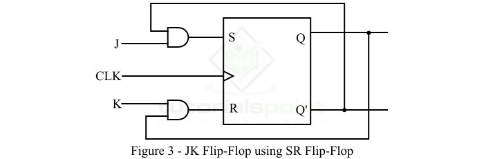
In this way, we can convert the SR flip-flop into JK flip-flop.