- Digital Electronics - Home
- Digital Electronics Basics
- Types of Digital Systems
- Types of Signals
- Logic Levels And Pulse Waveforms
- Digital System Components
- Digital Logic Operations
- Digital Systems Advantages
- Number Systems
- Number Systems
- Binary Numbers Representation
- Binary Arithmetic
- Signed Binary Arithmetic
- Octal Arithmetic
- Hexadecimal Arithmetic
- Complement Arithmetic
- Base Conversions
- Base Conversions
- Binary to Decimal Conversion
- Decimal to Binary Conversion
- Binary to Octal Conversion
- Octal to Binary Conversion
- Octal to Decimal Conversion
- Decimal to Octal Conversion
- Hexadecimal to Binary Conversion
- Binary to Hexadecimal Conversion
- Hexadecimal to Decimal Conversion
- Decimal to Hexadecimal Conversion
- Octal to Hexadecimal Conversion
- Hexadecimal to Octal Conversion
- Binary Codes
- Binary Codes
- 8421 BCD Code
- Excess-3 Code
- Gray Code
- ASCII Codes
- EBCDIC Code
- Code Conversion
- Error Detection & Correction Codes
- Logic Gates
- Logic Gates
- AND Gate
- OR Gate
- NOT Gate
- Universal Gates
- XOR Gate
- XNOR Gate
- CMOS Logic Gate
- OR Gate Using Diode Resistor Logic
- AND Gate vs OR Gate
- Two Level Logic Realization
- Threshold Logic
- Boolean Algebra
- Boolean Algebra
- Laws of Boolean Algebra
- Boolean Functions
- DeMorgan's Theorem
- SOP and POS Form
- POS to Standard POS Form
- Minimization Techniques
- K-Map Minimization
- Three Variable K-Map
- Four Variable K-Map
- Five Variable K-Map
- Six Variable K-Map
- Don't Care Condition
- Quine-McCluskey Method
- Min Terms and Max Terms
- Canonical and Standard Form
- Max Term Representation
- Simplification using Boolean Algebra
- Combinational Logic Circuits
- Digital Combinational Circuits
- Digital Arithmetic Circuits
- Multiplexers
- Multiplexer Design Procedure
- Mux Universal Gate
- 2-Variable Function Using 4:1 Mux
- 3-Variable Function Using 8:1 Mux
- Demultiplexers
- Mux vs Demux
- Parity Bit Generator and Checker
- Comparators
- Encoders
- Keyboard Encoders
- Priority Encoders
- Decoders
- Arithmetic Logic Unit
- 7-Segment LED Display
- Code Converters
- Code Converters
- Binary to Decimal Converter
- Decimal to BCD Converter
- BCD to Decimal Converter
- Binary to Gray Code Converter
- Gray Code to Binary Converter
- BCD to Excess-3 Converter
- Excess-3 to BCD Converter
- Adders
- Half Adders
- Full Adders
- Serial Adders
- Parallel Adders
- Full Adder using Half Adder
- Half Adder vs Full Adder
- Full Adder with NAND Gates
- Half Adder with NAND Gates
- Binary Adder-Subtractor
- Subtractors
- Half Subtractors
- Full Subtractors
- Parallel Subtractors
- Full Subtractor using 2 Half Subtractors
- Half Subtractor using NAND Gates
- Sequential Logic Circuits
- Digital Sequential Circuits
- Clock Signal and Triggering
- Latches
- Shift Registers
- Shift Register Applications
- Binary Registers
- Bidirectional Shift Register
- Counters
- Binary Counters
- Non-binary Counter
- Design of Synchronous Counter
- Synchronous vs Asynchronous Counter
- Finite State Machines
- Algorithmic State Machines
- Flip Flops
- Flip-Flops
- Conversion of Flip-Flops
- D Flip-Flops
- JK Flip-Flops
- T Flip-Flops
- SR Flip-Flops
- Clocked SR Flip-Flop
- Unclocked SR Flip-Flop
- Clocked JK Flip-Flop
- JK to T Flip-Flop
- SR to JK Flip-Flop
- Triggering Methods:Flip-Flop
- Edge-Triggered Flip-Flop
- Master-Slave JK Flip-Flop
- Race-around Condition
- A/D and D/A Converters
- Analog-to-Digital Converter
- Digital-to-Analog Converter
- DAC and ADC ICs
- Realization of Logic Gates
- NOT Gate from NAND Gate
- OR Gate from NAND Gate
- AND Gate from NAND Gate
- NOR Gate from NAND Gate
- XOR Gate from NAND Gate
- XNOR Gate from NAND Gate
- NOT Gate from NOR Gate
- OR Gate from NOR Gate
- AND Gate from NOR Gate
- NAND Gate from NOR Gate
- XOR Gate from NOR Gate
- XNOR Gate from NOR Gate
- NAND/NOR Gate using CMOS
- Full Subtractor using NAND Gate
- AND Gate Using 2:1 MUX
- OR Gate Using 2:1 MUX
- NOT Gate Using 2:1 MUX
- Memory Devices
- Memory Devices
- RAM and ROM
- Cache Memory Design
- Programmable Logic Devices
- Programmable Logic Devices
- Programmable Logic Array
- Programmable Array Logic
- Field Programmable Gate Arrays
- Digital Electronics Families
- Digital Electronics Families
- CPU Architecture
- CPU Architecture
Parity Bit Generator and Checker
In the field of digital electronics, it is very important to ensure the data integrity. For this purpose, we have two digital circuits namely, parity generator and parity checker. Both these circuits help us to detect and correct any kind of error in transmitted data.
Read this chapter to learn the basics of parity generator and parity checker, along with their types and applications.
What is a Parity Bit?
In digital signal processing, an additional bit either 0 or 1 is added to the original binary or digital code to detect and correct any kind of errors in the data that can occur during transmission. This additional bit is called a parity bit.
The addition of a parity bit to the original digital code makes the total number of 1s in the code either even or odd. Thus, on the basis of number 1s in the data, the parity can be classified into two types namely, even parity and odd parity.
If we add a 0 or a 1 to the original binary code and this makes the total number of 1s in the code an even number, then it is called an even parity.
On the other hand, if we add a parity bit i.e., 0 or 1 to the original binary code and this makes the total number of 1s in the code an odd number, then it is called an odd parity.
The parity bit is one of the simplest forms of error-detection technique used in digital electronics.
How Does the Parity Bit Work?
Let us now consider an example to understand how the parity bit works.
Suppose we have a decimal number say 5 and its BCD code is 0101. This code has total number of 1s are even, as it has two 1s.
In the case of even parity, we add a parity bit 0 to the original code to make the number of 1s an even number in the code.
Therefore, after adding even parity, we get 01010. Here, a 0 (parity bit) is added to the end of the original code.
In case, when we need to perform odd parity, then we add a 1 to end of the original code, we get 01011. Now, the total number of 1s in the code, including parity bit, is odd i.e., three 1s. This ensures that it is odd parity scheme.
The following table shows the odd and even parity bits for decimal digits from 0 to 9 −
| Decimal Digit | BCD | Even Parity | Odd Parity |
|---|---|---|---|
| 0 | 0 0 0 0 | 0 | 1 |
| 1 | 0 0 0 1 | 1 | 0 |
| 2 | 0 0 1 0 | 1 | 0 |
| 3 | 0 0 1 1 | 0 | 1 |
| 4 | 0 1 0 0 | 1 | 0 |
| 5 | 0 1 0 1 | 0 | 1 |
| 6 | 0 1 1 0 | 0 | 1 |
| 7 | 0 1 1 1 | 1 | 0 |
| 8 | 1 0 0 0 | 1 | 0 |
| 9 | 1 0 0 1 | 0 | 1 |
When a digital signal is received at the receiver end, a parity checker circuit generates an error signal if the total number of 1s is an odd number in an even parity scheme or an even number in an odd parity scheme.
The major limitation of parity bit error detection technique is that it can check only a single-bit error, but cannot check a multi bit error.
What is a Parity Generator?
A combinational logic circuit that can generate the parity bit according to the original digital code is known as a parity bit generator or parity generator.
The parity generator is used at the transmitter end and generate and add a parity bit the original code before transmission.
First, a parity generator reads the input data and calculates the parity bit accordingly. Once the parity bit is generated, it is added to the original data code. This gives an output code which is the original code with a newly generated parity bit.
Types of Parity Generators
Depending on the parity system used, there are two main types of parity generators −
- Even Parity Generator
- Odd Parity Generator
Let us discuss about even and odd parity generators in detail.
Even Parity Generator
An even parity generator is a type of parity generator in which the parity bit, either a 0 or a 1 is added to the original data so that the final digital code contains an even number of 1s, including the parity bit.
Therefore, we can state that total number of 1s in the output of an even parity generator including the parity bit is even.
In the case of an even parity generator −
- If a digital code contains an odd number of 1s, then the even parity generator will generate a 1 as parity bit to maintain the even parity.
- If a digital code already contains an even number of 1s, then the even parity generator will generate a 0 as the parity bit to maintain the even parity.
For example, consider a digital code 0110. This code already contains the even number of 1s. Hence, if it is input to an even parity generator, the output of the parity generator will be 01100. Where, the LSB 0 is a parity bit added by the even parity generator.
Similarly, consider another digital code 0111. In this case, the total number of 1s in the code is three (odd). If we input this code to an even parity generator, the generators output will be 01111, containing even number of 1s. Where, the LSB 1 is the parity bit.
Let us now design a 4-bit even parity generator. The following is the truth table of the 4-bit even parity generator −
| 4-Bit Code | Even Parity | |||
|---|---|---|---|---|
| A | B | C | D | P |
| 0 | 0 | 0 | 0 | 0 |
| 0 | 0 | 0 | 1 | 1 |
| 0 | 0 | 1 | 0 | 1 |
| 0 | 0 | 1 | 1 | 0 |
| 0 | 1 | 0 | 0 | 1 |
| 0 | 1 | 0 | 1 | 0 |
| 0 | 1 | 1 | 0 | 0 |
| 0 | 1 | 1 | 1 | 1 |
| 1 | 0 | 0 | 0 | 1 |
| 1 | 0 | 0 | 1 | 0 |
| 1 | 0 | 1 | 0 | 0 |
| 1 | 0 | 1 | 1 | 1 |
| 1 | 1 | 0 | 0 | 0 |
| 1 | 1 | 0 | 1 | 1 |
| 1 | 1 | 1 | 0 | 1 |
| 1 | 1 | 1 | 1 | 0 |
The Boolean expression of the 4-bit even parity generator can be obtained by simplifying its truth table, which is given below.
$$\mathrm{P \: = \: A \: \oplus \: B \: \oplus \: C \: \oplus \: D}$$
The logic circuit diagram of a 4-bit even parity generator is shown in the following figure.
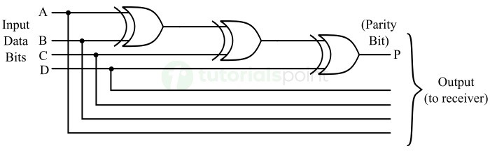
In this circuit, three XOR gates are connected together to add four data bits of the input code. The sum bit produced at the output will be the parity bit.
This is all about the even parity generator and its functioning.
Odd Parity Generator
A type of parity generator that adds a parity bit to a binary code so that the total number of 1s in the output code is an odd number, it is called an odd parity generator.
The output of an odd parity generator is a digital code that contains an odd number of 1s, including the parity bit.
In the case of an odd parity generator,
- If the original data contains an even number of 1s, then the odd parity generator adds a 1 as parity bit to the original code to maintain the odd parity.
- If the original data already contains an odd number of 1s, then the odd parity generator adds a 0 as parity bit to the original code to maintain the odd parity.
Let us understand the function of the odd parity generator with the help of examples.
Consider a 4-bit digital code that is 0110. This code has even number of 1s (two). Therefore, if we input this code to an odd parity generator, the generator will add a 1 and produces a code 01101 as output. This resulting code has odd number of 1s, including the parity bit, and ensuring the odd parity system.
Similarly, consider another 4-bit code that is 0111. This code already contains odd number of 1s i.e., three 1s. Therefore, the odd parity generator will add a 0 as parity bit to it and gives an output code as 01110 to ensure the odd parity system.
The following is the truth table of a 4-bit odd parity generator −
| 4-Bit Code | Odd Parity | |||
|---|---|---|---|---|
| A | B | C | D | P |
| 0 | 0 | 0 | 0 | 1 |
| 0 | 0 | 0 | 1 | 0 |
| 0 | 0 | 1 | 0 | 0 |
| 0 | 0 | 1 | 1 | 1 |
| 0 | 1 | 0 | 0 | 0 |
| 0 | 1 | 0 | 1 | 1 |
| 0 | 1 | 1 | 0 | 1 |
| 0 | 1 | 1 | 1 | 0 |
| 1 | 0 | 0 | 0 | 0 |
| 1 | 0 | 0 | 1 | 1 |
| 1 | 0 | 1 | 0 | 1 |
| 1 | 0 | 1 | 1 | 0 |
| 1 | 1 | 0 | 0 | 1 |
| 1 | 1 | 0 | 1 | 0 |
| 1 | 1 | 1 | 0 | 0 |
| 1 | 1 | 1 | 1 | 1 |
The Boolean expression of the 4-bit odd parity generator is,
$$\mathrm{P \: = \: \overline{A \: \oplus \: B \: \oplus \: C \: \oplus \: D}}$$
The following figure depicts the logic circuit diagram of the 4-bit odd parity generator.
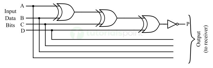
In this circuit, three XOR gates are connected together to add the four bits of the input data and the sum bit is then complemented to obtain the odd parity bit.
This is all about the even parity generator and odd parity generator. Both of these types of parity generators are used in digital systems to implement different types of parity systems depending on the needs of the applications.
Parity generators are extensively used in digital communication and storage systems to check errors that can occur during transmission of data.
What is a Parity Checker?
A combinational circuit that checks and verifies the correctness of the transmitted data by analyzing the parity bit is called a parity checker. The main function of a parity checker is to detect errors that can occur during data transmission.
Parity checkers are used at the receiver end of the communication channel. It receives the transmitted data from the communication channel. This data includes the original message code and the parity bit.
After that, the parity checker counts the number of 1s in the data code and compares this number with the expected code to determine whether there is any error or not. If there is any error in the received data, the parity checker takes an appropriate action like request to retransmit the data.
The parity checker is an essential component in the digital communication systems to ensure the correctness and integrity of data. It also provides a simple and effective method for error detection.
Types of Parity Checkers
Depending on the parity system used, there are two main types of parity checkers −
- Even Parity Checker
- Odd Parity Checker
Let us discuss each type of parity checker in detail.
Even Parity Checker
The type of parity checker that verifies whether the received data is correct as per the even parity system is called an even parity checker.
The even parity checker counts and verifies that the received data contains an even number of 1s, including the parity bit.
Thus, in the case of an even parity checker,
- If the number of 1s in the received data is even, then it is considered that the data is error free.
- If the number of 1s in the received data is odd, then the parity checker shows that the data contains some error.
How Does an Even Parity Checker Work?
Let us understand the even parity checking with the help of an example.
Consider a 4-bit digital code 00110 (having 0 as parity bit at LSB position), this code is received by the even parity checker. The parity checker will count the number of 1s in the code which is even (two). Thus, the parity checker shows that it is an error free code, where LSB 0 is the parity bit.
Similarly, consider another 4-bit message code 01011 with a parity bit at the LSB place. This code contains odd number of 1s (three 1s). Hence, the even parity checker will show that the code has some error.
Let us now implement a 4-bit even parity checker whose truth table is shown below −
| 4-Bit Code with Parity | Even Parity Check | ||||
|---|---|---|---|---|---|
| A | B | C | D | P | CP |
| 0 | 0 | 0 | 0 | 0 | 0 |
| 0 | 0 | 0 | 0 | 1 | 1 |
| 0 | 0 | 0 | 1 | 0 | 1 |
| 0 | 0 | 0 | 1 | 1 | 0 |
| 0 | 0 | 1 | 0 | 0 | 1 |
| 0 | 0 | 1 | 0 | 1 | 0 |
| 0 | 0 | 1 | 1 | 0 | 0 |
| 0 | 0 | 1 | 1 | 1 | 1 |
| 0 | 1 | 0 | 0 | 0 | 1 |
| 0 | 1 | 0 | 0 | 1 | 0 |
| 0 | 1 | 0 | 1 | 0 | 0 |
| 0 | 1 | 0 | 1 | 1 | 1 |
| 0 | 1 | 1 | 0 | 0 | 0 |
| 0 | 1 | 1 | 0 | 1 | 1 |
| 0 | 1 | 1 | 1 | 0 | 1 |
| 0 | 1 | 1 | 1 | 1 | 0 |
| 1 | 0 | 0 | 0 | 0 | 1 |
| 1 | 0 | 0 | 0 | 1 | 0 |
| 1 | 0 | 0 | 1 | 0 | 0 |
| 1 | 0 | 0 | 1 | 1 | 1 |
| 1 | 0 | 1 | 0 | 0 | 0 |
| 1 | 0 | 1 | 0 | 1 | 1 |
| 1 | 0 | 1 | 1 | 0 | 1 |
| 1 | 0 | 1 | 1 | 1 | 0 |
| 1 | 1 | 0 | 0 | 0 | 0 |
| 1 | 1 | 0 | 0 | 1 | 1 |
| 1 | 1 | 0 | 1 | 0 | 1 |
| 1 | 1 | 0 | 1 | 1 | 0 |
| 1 | 1 | 1 | 0 | 0 | 1 |
| 1 | 1 | 1 | 0 | 1 | 0 |
| 1 | 1 | 1 | 1 | 0 | 0 |
| 1 | 1 | 1 | 1 | 1 | 1 |
Here, the bits ABCD represents the original digital code and P is the parity bit.
In this truth table, if CP = 1, there will be an error in the received code. If CP = 0, there is no error in the received code.
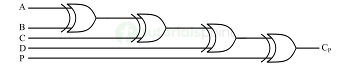
The Boolean expression of the 4-bit even parity checker is,
$$\mathrm{C_{P} \: = \: A \: \oplus \: B \: \oplus \: C \: \oplus \: D \: \oplus \: P}$$
The logic circuit diagram of the 4-bit even parity checker is shown in the following figure.
Odd Parity Checker
An odd parity checker is a combinational logic circuit that checks and verifies whether the received data is correct as per the odd parity system.
An odd parity checker counts and confirms that the received data contains odd number of 1s including the parity bit.
In the case of an odd parity checker,
- If the number of 1s in the received code is odd, there is no error in the code.
- If the number of 1s in the received code is even, this represents an error in the code that might be occurred during transmission.
For example, consider a 4-bit data code 01101 (LSB 1 is the parity bit). In this code, the number of 1s are odd (three). Thus, the odd parity checker will show that the code is error free.
Similarly, consider another 4-bit data code 01100 (LSB 0 is the parity bit). This code contains the even number of 1s i.e., only two 1s are there. In this case, the odd parity checker will show that the code has an error.
Let us now implement a 4-bit odd parity checker whose truth table is shown below.
| 4-Bit Code with Parity | Odd Parity Check | ||||
|---|---|---|---|---|---|
| A | B | C | D | P | CP |
| 0 | 0 | 0 | 0 | 0 | 1 |
| 0 | 0 | 0 | 0 | 1 | 0 |
| 0 | 0 | 0 | 1 | 0 | 0 |
| 0 | 0 | 0 | 1 | 1 | 1 |
| 0 | 0 | 1 | 0 | 0 | 0 |
| 0 | 0 | 1 | 0 | 1 | 1 |
| 0 | 0 | 1 | 1 | 0 | 1 |
| 0 | 0 | 1 | 1 | 1 | 0 |
| 0 | 1 | 0 | 0 | 0 | 0 |
| 0 | 1 | 0 | 0 | 1 | 1 |
| 0 | 1 | 0 | 1 | 0 | 1 |
| 0 | 1 | 0 | 1 | 1 | 0 |
| 0 | 1 | 1 | 0 | 0 | 1 |
| 0 | 1 | 1 | 0 | 1 | 0 |
| 0 | 1 | 1 | 1 | 0 | 0 |
| 0 | 1 | 1 | 1 | 1 | 1 |
| 1 | 0 | 0 | 0 | 0 | 0 |
| 1 | 0 | 0 | 0 | 1 | 1 |
| 1 | 0 | 0 | 1 | 0 | 1 |
| 1 | 0 | 0 | 1 | 1 | 0 |
| 1 | 0 | 1 | 0 | 0 | 1 |
| 1 | 0 | 1 | 0 | 1 | 0 |
| 1 | 0 | 1 | 1 | 0 | 0 |
| 1 | 0 | 1 | 1 | 1 | 1 |
| 1 | 1 | 0 | 0 | 0 | 1 |
| 1 | 1 | 0 | 0 | 1 | 0 |
| 1 | 1 | 0 | 1 | 0 | 0 |
| 1 | 1 | 0 | 1 | 1 | 1 |
| 1 | 1 | 1 | 0 | 0 | 0 |
| 1 | 1 | 1 | 0 | 1 | 1 |
| 1 | 1 | 1 | 1 | 0 | 1 |
| 1 | 1 | 1 | 1 | 1 | 0 |
In this truth table, the bits ABCD represents the original binary code and P is the parity bit.
From this truth table, we can observe that if CP = 1, the code contains an even number of 1s and hence, there is an error occurred in the code during transmission.
If CP = 0, the code contains odd number of 1s which represents that the code is error free.
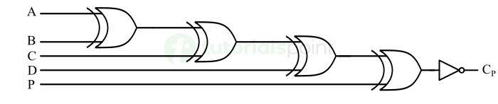
The Boolean expression of the 4-bit odd parity checker is given here,
$$\mathrm{C_{P} \: = \: \overline{A \: \oplus \: B \: \oplus \: C \: \oplus \: D \: \oplus \: P}}$$
The logic circuit diagram of this 4-bit odd parity checker is depicted in the following figure.
IC 74180 9-Bit Parity Generators/Checkers
A parity generator/checker IC is a small device which is used to detect errors in data streams transmitted over a communication channel. There are several different parity generator/checker IC available in the market, but one most commonly used is 74180 IC.
The 74180 Parity Generator/Checker IC is a 9-bit parity generator or checker device that is used in high-speed data transmission systems to detect errors.
The pin diagram of the parity generator/checker IC 74180 is shown in the following figure.
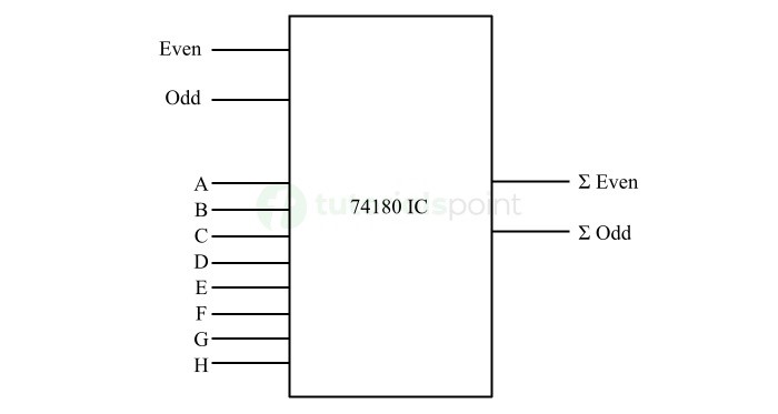
It consists of eight input lines labeled from A to H, two cascading input lines labeled as "even" and "odd", and two output lines designated as "even sum" and "odd sum".
Depending on the operating mode selected, the IC 74180 can operate as either a parity generator or a parity checker.
Let us now consider an example to understand the how does the parity generator/checker IC work?
If the IC 74180 is operated as an even parity checker and there is a parity error in the received data. In this case, the output "even sum" will be low and the output "odd sum" will be high.
If the IC 74180 is operated as an odd parity checker and an error occurs in the data stream. The output "odd sum" will be low and the output "even sum" will be high.
This is all about parity generator or checker IC 74180. Let us now discuss the applications of parity generators/checkers.
Applications of Parity Generators and Checkers
In digital systems, like digital communication and storage systems, the parity generator and checker are essential components that provide a robust method for error detection and correction in transmitted and retrieved data streams. Thus, parity generator/checker helps to ensure data integrity, reliability, and security of digital data.
The following examples illustrate the applications of parity generators and checkers in various digital electronic applications −
- In digital communication systems, parity generators and checkers are used to ensure integrity and accuracy of the transmitted and received data. Parity generators and checkers help to detect errors in the data that can be caused due to noise and interference during transmission over communication channels.
- Parity generators and checkers are used in storage systems like RAM and ROM to detect errors in the data stored and retrieved.
- In digital networking, parity generators and checkers are used to improve reliability of data transmission and verify the correctness of the transmitted data.
- Parity generators and checkers are used in industrial automation and control systems to ensure accurate and reliable operation of industrial systems.
- Parity generators and checkers are also used in medical equipment used to diagnose and monitor patients health and avoid any kind errors in medical reports and diagnosis data.
Conclusion
A parity generator is a combinational logic circuit used to generate and add a parity to the input or transmitted data, while a parity checker is also a combinational circuit used to verify the correctness of received data.
Parity generators are used in the transmitter circuit and parity checkers are used in the receiver circuit. Both these circuits are collectively used to ensure the reliability, integrity, and accuracy of data in various digital systems.